Good EMC Design Guidelines
These design guidelines generally offer good advice, though they are not necessarily the best advice in every situation.
Circuit Board Layout (Component Selection and Placement)
Connectors should be located on one edge or on one corner of a board.
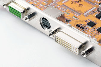 Locating the connectors on one edge of the board makes it much easier to hold them all to the same reference potential. This is extremely important for boards with high-frequency components that will not be housed in a shielded enclosure. Some designs require that connectors be located on different sides of the board. In these cases, every effort should be made to avoid placing high-frequency circuits between any two connectors.
When placing high-frequency circuits between connectors is unavoidable, a metal enclosure and filtering to chassis ground is generally necessary to keep the board from being able to drive common-mode currents onto the attached cables.
A device on the board that communicates with a device off the board through a connector should be located as close as possible (e.g., within 2 cm) to that connector.
This is another way of saying keep your I/O traces short. If an I/O trace comes too far onto the board, it is more likely to couple noise to or from other circuits on the board.
All off-board communication from a single device should be routed through the same connector.
Common-mode currents are much easier to control in wires that are part of the same cable bundle.
Components not connected to an I/O net should be located at least 2 cm away from I/O nets and connectors.
Why 2 cm? The minimum distance will depend on the situation. However, it does make sense to keep non-I/O circuits away from the I/O nets, since noise is easily coupled on or off the board through the I/O.
Clock drivers should be located adjacent to clock oscillators.
We could probably take this one step further and say that any component (such as a clock oscillator) that communicates exclusively with another component (such as a clock driver) should be located close to that component, especially if the communication is a high-frequency signal.
Circuit Board Layout (Trace Routing)
A trace with a propagation delay of more than half the transition time of the signal it carries must have a matched termination.
Don't use a matched termination unless the risetime has already been slowed as much as possible, and the trace length has been shortened as much as possible. Matched terminations are undesirable because they draw more power and make it more difficult to control risetimes. However, they are generally necessary for signal integrity and EMC when the trace delay is greater than the transition time.
No trace unrelated to I/O should be located between an I/O connector and the device(s) sending and receiving signals using that connector.
I/O traces provide relatively easy paths for noise to get on or off the board. Great care should be taken to limit unintentional coupling to or from these traces.
All power planes and traces should be routed on the same layer.
This is almost always a good idea. It ensures that different voltage planes don't overlap and helps to minimize noise coupling between power buses. An exception might be made for plane pairs such as plus and minus 12 V, where it is generally best to maintain balance by routing identical planes on different layers.
Power planes on the same layer must have at least a 3-mm gap between them.
3 mm? Maybe. It is true, however, that a gap between two power planes must be equal to or greater than the spacing between the power planes and the ground planes. Otherwise, there is relatively little high-frequency isolation between these planes.
Critical nets should be routed at least 2X from the board edge, where X is the distance between the trace and its return current path.
Traces routed too close to the board edge exhibit poor field containment and more easily couple to external cables and other objects.
Signals with high-frequency content should not be routed beneath components used for board I/O.
This is a recurring theme. "Keep noisy signals and components away from the I/O".
Differential pairs radiate much less than single-ended signals even when the traces in the pair are separated by many times their distance above a ground plane. However, an imbalance in the pair can result in radiation comparable to an equivalent single-ended signal.
If we were to re-word this in the form of a design guideline, it might say, "Be sure to maintain balance when routing your differential signals in order to ensure that you derive the noise-canceling benefits of a differential signal."
The length of high-frequency nets should be minimized.
This is another way of saying, "Control your loop areas."
The number of vias in high-frequency nets should be minimized.
Don't allow your most critical nets to make too many layer transitions. Some energy is lost with each transition, and it's more difficult to maintain control of current return paths.
On a board with power and ground planes, no traces should be used to connect to power or ground. Connections should be made using a via adjacent to the power or ground pad of the component.
Traces on power or ground take up space on the board and add inductance to the connection. There is generally no good reason to have these traces, so they should be eliminated.
Unused digital signal input pins on an active device should be tied high or low (i.e., not left floating).
Small amounts of noise coupled to floating inputs may cause the input to change state. Even if the logic ignores the state of that input, one switching input can trigger the switching of dozens of internal logic gates. This can put noise on the power bus. Unless you are sure that a floating input can't be toggled by coupled noise, it is a good practice to tie it either high or low.
Circuit Board Decoupling Guidelines
Power Bus Decoupling Guidelines for Printed Circuit Boards without Power Planes
Power Bus Decoupling Guidelines for Printed Circuit Boards with Closely Spaced Power Distribution Planes
Power Bus Decoupling Guidelines for Printed Circuit Boards with Widely Spaced Power Distribution Planes
Chip Level Guidelines
Be sure your chip design has adequate on-chip decoupling.
Insufficient on-chip decoupling is often responsible for EMI and signal integrity problems. Noise on the chip's power bus tends to appear on all of the pins connected to the device. This effectively turns all of the traces attached to the device into high-speed lines. Unless all traces are carefully routed and terminated, EMI problems are likely to occur. Package-level and board-level decoupling cannot compensate for inadequate chip-level decoupling.
Do not segment ground domains within a chip.
For the same reasons, you shouldn't segment ground domains on a board.
There is little difference (from an EMI standpoint) between plastic and metal chip packages unless a metal chip package is well-connected to a chassis or PCB ground plane.
This is generally true.
It is important to have as many ground bonds as possible, evenly distributed around a chip die.
Ground on a chip is relatively high impedance (mostly resistance). Take advantage of the lower resistance available off-chip to maintain a single reference potential.
Every power or signal connection should be located near its corresponding power or signal return connection, never on the opposite side of the chip.
Don't let a poor pin assignment force your chip design to pull power or signal currents all the way across the chip.
Control slew-rate, especially on I/O. Transition times that are a little faster than necessary significantly increase the amount of energy at high frequencies.
This will help reduce crosstalk on the chip as well as reduce EMI problems with the boards that employ this chip.