Introduction to Imbalance Difference Modeling
It is the most significant development in the field of electromagnetic compatibility in the past 20 years, and yet many EMC engineers are unaware of it. The following article provides a brief overview of what Imbalance Difference Modeling is, and the amazing impact it has had on our ability to understand and model sources of electromagnetic radiation.
Point #1: It's the Common-Mode Current
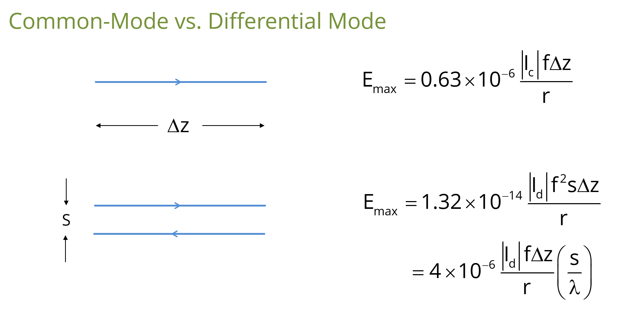
When an electronic product produces radiated emissions that exceed regulatory requirements, it is virtually always due to common-mode currents. These typically are currents that are inadvertently induced on cables and/or various large structures in the product. At any given instant in time, common-mode currents flow in one direction, creating fields that are not canceled by currents flowing in the opposite direction on a nearby conductor.
Differential-mode currents (i.e., currents flowing in opposing directions on closely spaced conductors) do not radiate efficiently. For example, on a standard CAT5 twisted wire pair, just 5 μA of common-mode current at 100 MHz produces a stronger radiated field than 100 mA of differential-mode signal current flowing on the same cable.
When it comes to modeling or estimating radiated emissions from a product, differential-mode signal currents can usually be neglected. If none of the power in a differential-mode signal is converted to common-mode, the signal will generally not result in measurable radiated emissions.
It’s important to note that any current flowing out on one conductor and back on a nearby conductor is differential-mode current, as we’ve defined it here. So while the currents associated with differential signals are certainly differential-mode, the currents associated with single-ended signals (e.g., flowing on circuit board traces over a ground plane) are also differential-mode. In a well-designed system, all of the high-frequency signal currents flow to the load on one conductor and back to the source on a nearby conductor. To the extent that these currents are equal and opposite, they do not contribute significantly to the radiated emissions. Only the common-mode currents produce significant radiated emissions.
Point #2: Common-Mode Current is the Result of Mode Conversion
If all of the signals are effectively differential-mode, where do the radiated emissions come from? The simple answer is: mode conversion. Some of the power in a differential-mode signal propagating on a transmission line is converted to common-mode if, and only if, the signal experiences a change in electrical balance. The electrical balance is essentially a measure of the relative impedance to ground of each of the two conductors in the transmission line. For example, a twisted-wire pair is a balanced transmission line because both conductors have the same impedance with respect to whatever has been identified as “ground.” On the other hand, a circuit board trace over a wide plane is a very unbalanced transmission line, because the plane has a much different geometry than the trace.
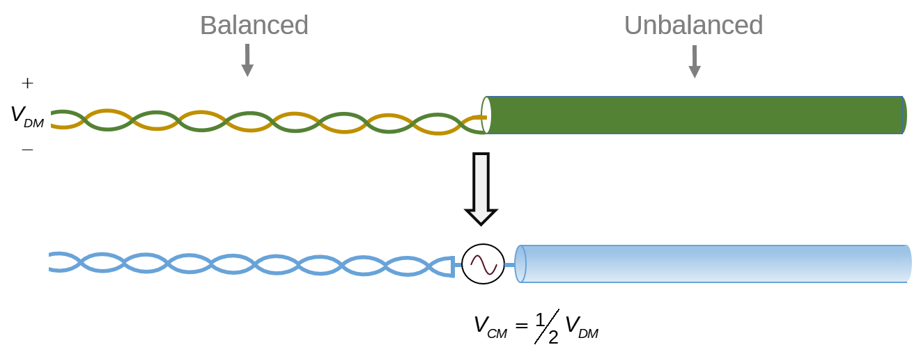
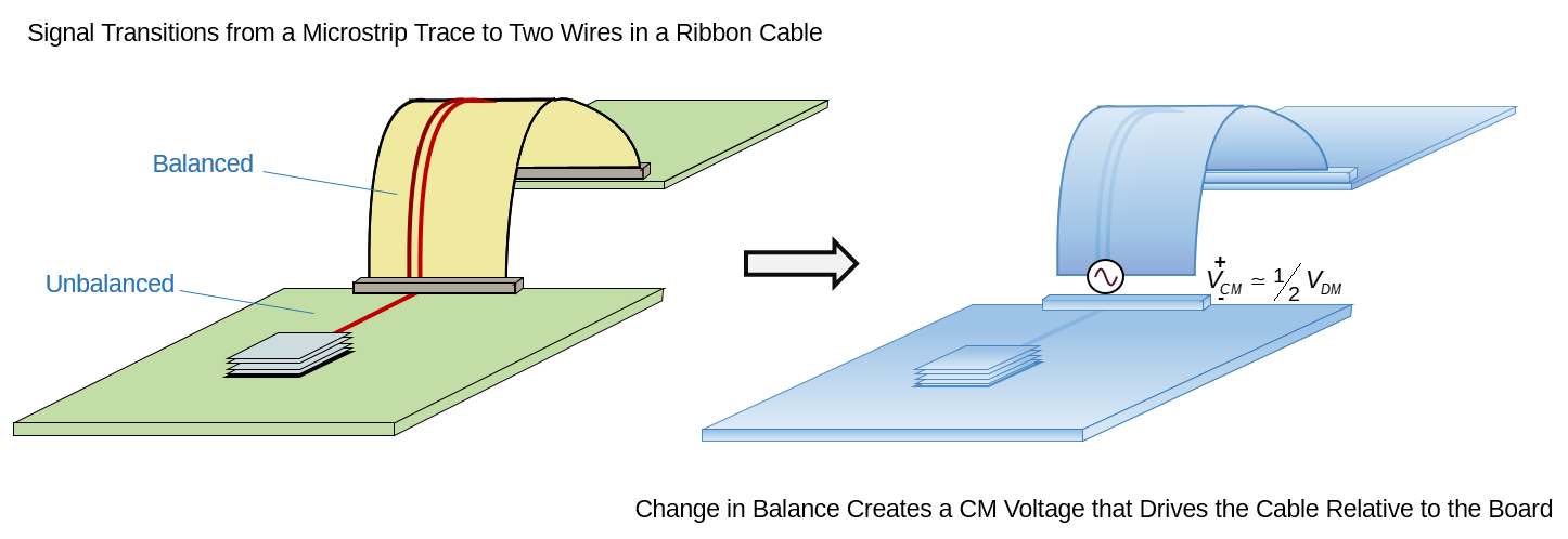
Differential-mode signals propagate equally well on balanced or unbalanced transmission lines without mode conversion. Mode conversion occurs only when the signal experiences a change in the balance of the transmission line. For example, a signal propagating on a trace over a wide plane that transitions to a twisted wire pair when it leaves the board will experience significant mode conversion. In this case, a common-mode voltage would be developed at the connection that would drive the board relative to the cable. This would result in common-mode currents capable of generating significant radiated emissions.
Point #3: Imbalance Difference Modeling Quantifies Mode Conversion
Common-mode and differential-mode propagation on unbalanced transmission lines was described by Uchida as early as 1967 for three-conductor systems where one of the conductors was identified as ground [1]. Uchida showed that the two orthogonal modes can be concisely defined as
(1) (2) (3) (4)where V1 and V2 are the voltages on conductors 1 and 2 with respect to ground, and I1 and I2 are the currents on conductors 1 and 2, respectively. VCM and VDM are the common-mode and differential-mode voltages. ICM and IDM are the common-mode and differential-mode currents. The h in these equations is called the current division factor, or imbalance factor. It represents the fraction of the current that flows on conductor 1 when both conductors are driven with a common-mode source (i.e., driven with the same voltage relative to ground). (1 - h) is the fraction of the current that flows on conductor 2. For a known conductor geometry, h can be calculated as
(5)where Z1 and Z2 are the characteristic impedances of the transmission lines formed by conductors 1 and 2 with ground, respectively.
In 2000, Watanabe [2] proposed applying this concept to two-conductor transmission lines where the ground was essentially at infinity. He showed that a common-mode voltage was developed whenever a differential-mode signal propagating in a two-conductor transmission line experienced a change in the imbalance factor. This common-mode voltage is given by the relatively simple expression,
(6)where VDM is the differential-mode voltage at the point where the imbalance changes, and Δh is the change in the imbalance factor at that point. (With the ground at infinity, the characteristic impedances in the expression for h above are replaced with self-capacitances or self-partial-inductances per unit length, which are readily calculated using 2D field solvers.)
In the nearly two decades since [2] was published, many researchers have used this concept (often referred to as Imbalance Difference Theory or Imbalance Difference Modeling) to model a wide variety of problems applicable to electromagnetic compatibility. And while the expression for calculating the common-mode voltage shown above was initially considered to be an approximate expression, it yielded extremely accurate results. Eventually, it was shown that the expression is exact and that mode conversion occurs only when there is a change in the electrical balance of the transmission line [3].
Point #4: Imbalance Difference Modeling (IDM) is Extremely Powerful and Intuitive
The development of Imbalance Difference Modeling is arguably the most significant advancement in the field of electromagnetic compatibility in the past 20 years. It has enabled the accurate modeling of complex circuit board and wire harness structures, using numerical modeling techniques. At the same time, it provides an intuitive basis for making basic EMC design decisions. The three sections below summarize how imbalance difference modeling is used to:
- Enable precise numerical modeling of complex circuit board and cable structures,
- Perform simple worst-case modeling to guarantee compliance with emissions requirements, and
- Provide basic EMC design guidance for circuit and system designers.
IDM for precise modeling of complex circuit board and wire harness structures
Suppose you want to model something as simple as the radiated emissions from a circuit board trace over a ground plane. One method would be to enter the circuit board geometry into a full-wave field solver. It would have to be a powerful field solver though, because even this simple geometry has features that create challenges for full-wave codes. For example, the trace is closely spaced to the plane and there is an interceding dielectric. Also, the trace and the board dimensions may be relatively large while the dielectric thickness is very small. If you increase the complexity of the model (e.g., by adding more traces, attached cables, heatsinks, etc.), the problem becomes much worse. For these reasons and others, full-wave models of complex circuit board structures rarely yield useful results.
Now, suppose we recognize that the differential-mode signal currents do not contribute significantly to the overall radiated emissions. The only parts of the structure that really need to be modeled are the common-mode sources and the objects that carry common-mode currents. Once the signal voltages have been determined, imbalance difference modeling can tell us exactly where the common-mode sources are.
For a trace whose width and height above the plane don’t change, there are at most two common-mode sources: one at the source end and one at the load end. From the differential-mode signal voltage and the imbalance difference, we can calculate the common-mode voltages that drive the structure. At this point, we can eliminate the trace structure and the dielectric, because they have very little impact on the common-mode currents. The remaining model elements are relatively easy to model with a full-wave code. Perhaps more importantly, the parameters that have a significant impact on the radiated emissions are easily identified. This technique is described fairly concisely in [4].
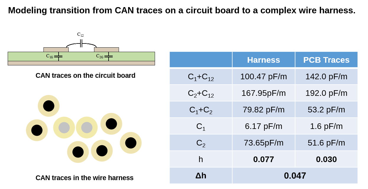
Complex wiring harnesses can be modeled using the same general approach. The differential-mode voltages and currents in the harness can be obtained using relatively simple and accurate transmission line modeling tools. However, it’s the common-mode current on the harness that is important for modeling radiated emissions and immunity.
Imbalance difference modeling allows us to simplify the model greatly. First, transmission line codes and/or static electric field codes are used to model the harness in order to obtain the differential-mode voltages and imbalance factors. Since these are 2D calculations, complex harness geometries and materials do not present a significant challenge. These values are then used to determine the location and amplitude of the common-mode voltage sources that drive common-mode current onto the harness (or convert common-mode currents to differential-mode noise). In a 3D full-wave simulation, the entire harness can then be modeled using a solid wire with the appropriate common-mode sources. The complexity of the harness geometry is eliminated with no significant reduction in the accuracy of the model result.
The same technique can be applied to the analysis of connectors. Electrical balance is often overlooked in connector design, but it is the most important factor (actually, the only factor) affecting differential-mode to common-mode conversion within or due to the connector. Imbalance Difference Modeling can be used to quickly determine exactly how much common-mode voltage will be developed across a connector, even when the connector geometry is complicated, and multiple signals pass through it.
IDM for simple worst-case analysis of circuit board and wire harness structures
In the course of designing or reviewing an electronic system for potential EMC issues, it is unlikely that one would perform the types of detailed modeling described above. Nevertheless, imbalance difference modeling calculations are an important part of an EMC design review.
During a design review, we don’t numerically model specific configurations because EMC testing is not about how specific configurations perform. Designing to meet EMC requirements is all about ensuring that worst-case configurations will meet the requirements. For example, an EMC engineer might recognize that driving two cables relative to each other with more than about 1 mV of noise could cause a product to fail its radiated emissions requirement. A full-wave model of the structure wouldn’t be helpful, because small variations in the test configuration could make significant differences in the radiated emissions. Furthermore, the precise configuration used in the test is generally undefined during product development, and may vary significantly from one test lab to another.
Imbalance Difference Modeling can be applied to determine the amount of common-mode voltage driving any two cables or large metallic structures based on the differential-mode signal amplitudes and transmission line geometries. It usually isn’t even necessary to calculate the precise imbalance factors, because a worst-case analysis can be done using worst-case numbers for the change in the imbalance. For example, the worst-case imbalance difference transitioning from a microstrip trace (very unbalanced) to an unshielded ribbon cable (pretty balanced) would be Δh = 1/2.
A similar analysis can be quickly conducted to determine the maximum voltage driving complex wire harnesses, or the worst-case common-mode voltage generated as signals pass through a connector. Simply ensuring that the worst-case common-mode voltages are well below the threshold tied to a particular radiated emissions or immunity requirement ensures that any given cable or connector will not be the source of an EMC test failure.
Prior to the development of Imbalance Difference Modeling, these kinds of calculations were much more difficult. Common-mode voltages were generally obtained using relatively complex models involving partial self and partial mutual inductances. These models were approximations; they were very difficult to apply without computer modeling, and they couldn’t be applied at all to complex wire harness geometries. Imbalance Difference Modeling has greatly simplified the process, making it much easier to perform during a design review and enabling EMC engineers to guarantee compliance with radiated emission requirements.
IDM for intuitive EMC design guidance
Circuit board and system designers whose primary focus is not EMC are not likely to perform imbalance difference calculations as a normal part of the design process. Nevertheless, they can benefit greatly by being familiar with the general concepts. A good rule-of-thumb to follow when designing any electrical signal path is: If the signal is balanced, stay balanced. If the signal is unbalanced, stay unbalanced. In other words, differential signals should be routed on balanced transmission lines and terminated in balanced loads. Single-ended sources should be routed on unbalanced transmission lines and terminated in unbalanced loads.
Most of the transmission lines routinely used in electronic systems are either very balanced (e.g., wire pairs or differential traces) or very unbalanced (e.g., coaxial cables or microstrip traces). When a balanced signal encounters an unbalanced transmission line, a common-mode excitation is developed that drives the transmission line with roughly half the differential-mode signal voltage. For some non-critical, low-frequency signals, this may be fine, but it should be a conscious design decision. Significant radiation and immunity problems can result when nobody is paying attention to the electrical balance of a signal path.
Point #5: This Has Only Been a Brief Introduction
This brief introduction to Imbalance Difference Modeling is intended to provide a general understanding of the concept and its importance in the field of electromagnetic compatibility. But a brief introduction can’t possibly equip someone to take full advantage of this technique.
A large number of papers have been written that apply imbalance difference modeling to the analysis of problems of interest to EMC engineers and electronic system designers (e.g., see the Imbalance Difference Modeling Bibliography). The reader is encouraged to explore the topic further by reviewing the papers that cover applications likely to be of interest.
References
- H. Uchida, Fundamentals of Coupled Lines and Multiwire Antennas, Sasaki Printing and Publishing, pp. 37-39, 1967.
- T. Watanabe, O. Wada, T. Miyashita, and R. Koga, “Common-Mode-Current Generation Caused by Difference of Unbalance of Transmission Lines on a Printed Circuit Board with Narrow Ground Pattern,” IEICE Trans. Commun., vol. E83-B, no. 3, pp. 593–599, Mar. 2000.
- L. Niu and T. Hubing, “Rigorous Derivation of Imbalance Difference Theory for Modeling Radiated Emission Problems,” IEEE Trans. Electromagn. Compat., vol. 57, no. 5, Oct. 2015, pp. 1021-1026.
- C. Su and T. H. Hubing, “Imbalance Difference Model for Common-Mode Radiation from Printed Circuit Boards,” IEEE Trans. Electromagn. Compat., vol. 53, no. 1, pp. 150–156, Feb. 2011.