Circuit Board Decoupling
A sudden change in the amount of current drawn by an electronic device can cause a momentary dip or spike in the voltage on the power distribution bus. This voltage variation can impact the operation of other devices on the same power bus. The goal of power bus decoupling is to reduce power bus noise coupling between active circuits.
In many ways, power bus decoupling is similar to power bus filtering. However, most forms of power bus filtering impede the flow of high-frequency currents on the power bus. The focus of power bus decoupling is to meet the high-frequency current demands of active devices without allowing the power bus voltage to vary significantly.
Consider the printed circuit board illustrated below. A low impedance, 3.3-volt source supplies power to two active components on a printed circuit board. Assuming the resistance of the traces and connections is negligible, the voltage appearing at the pins of both components is approximately 3.3 volts. However, a sudden change in the current drawn by one of the components can cause the voltage delivered to the board to momentarily drop due to the connection inductance.
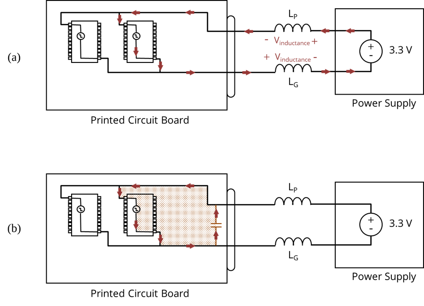
For example, assume the connection between the power source and the board was made using a 30-cm long twisted wire pair with an inductance per unit length of 5 nH/cm. If the current drawn by the board changes from 1.00 amperes to 1.15 amperes in 20 ns, the voltage seen by both components on the board would drop momentarily. The average voltage during this transition would be,
A larger or more sudden current change would cause the voltage to drop even more. This voltage transient would be observed by every component on the board and could result in data errors or, in severe cases, damage to the components.
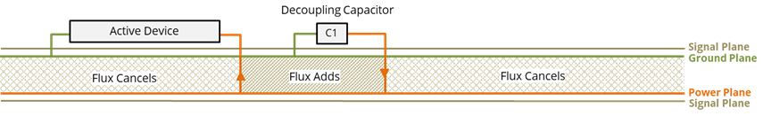
One solution to this problem is to place a capacitor on the board in parallel with the power source, as shown in (b). The capacitor stores charge on the board and supplies current in response to any change in voltage across its terminals. Therefore, the capacitor helps to stabilize the voltage on the board. Capacitors with both terminals connected to different reference voltages are called decoupling capacitors, because they reduce common impedance coupling between components sharing the same power bus.
Power Bus Impedance
The ratio of the power bus voltage change to the change in current supplied by the power bus is the power bus impedance,
If we know how much current we need to supply to a board at any given frequency, and we know how much noise voltage we are willing to tolerate, we can calculate the maximum allowable power bus impedance at that frequency. For example, if we plot the power bus impedance of the circuit above as a function of frequency, we see that the impedance increases with frequency due to the power bus inductance, as shown by the solid line in the figure below.
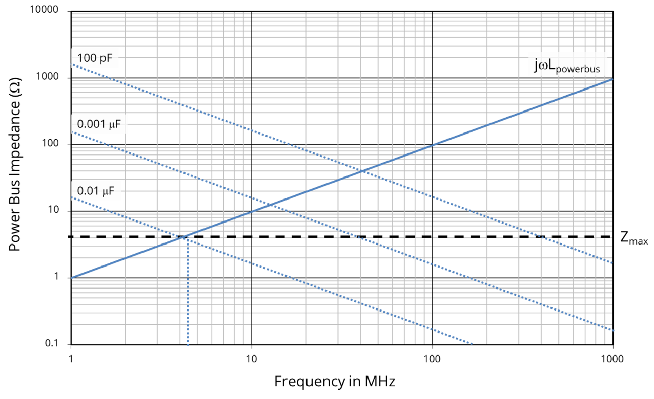
If we were willing to tolerate no more than 0.033 volts of power bus noise, but we needed to be able to supply at least 8 mA of current at any frequency up to 25 MHz, the maximum allowable power bus impedance would be,
The horizontal dashed line in the plot above indicates the maximum allowable power bus impedance. Note that power bus impedance exceeds the maximum allowable impedance at frequencies greater than,
In other words, drawing 8 mA of current from the power bus at any frequency above 4.4 MHz would cause the power bus noise to exceed the specification.
Suppose that we add a decoupling capacitor to the circuit as indicated in (b). The impedance of the power bus now consists of the bus inductance and the decoupling capacitance in parallel. The impedance of the capacitor for several possible capacitance values is indicated by the dotted lines in the above plot.
As indicated in the plot, this application requires a capacitor with a value of at least 0.01 μF to meet the power bus noise specification. Larger values of capacitance are even better, but smaller values do not supply enough current at the lower frequencies.
At high frequencies, the dotted lines in the plot suggest that the capacitors are more than adequate. However, the connection between the active device and the decoupling capacitor also has a loop area, as indicated in the figure below. We need to model the connection inductance associated with the decoupling capacitor to adequately characterize the high-frequency behavior of the power bus. In this case, approximating the connection as a square 3-cm x 3-cm loop, we estimate the inductance of the connection to be approximately Lglobal = 40 nH. The subscript global indicates that this capacitor has approximately the same inductance to all the active devices on the board.
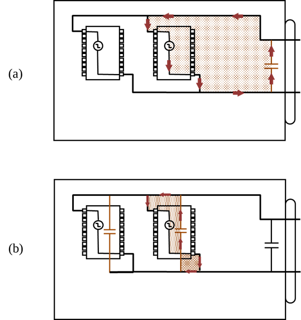
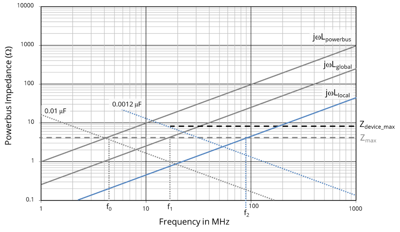
The impedance of the connection inductance is included in the plot below. Since this inductance is in series with the active device, the overall power bus impedance is determined by adding this impedance to the impedance of the rest of the bus. Note that the effect of adding the global decoupling capacitor to this circuit was to increase the maximum effective frequency of the power bus from f0 = 4.4 MHz to f1 = 16 MHz. Also note that the new maximum frequency is determined entirely by the connection inductance of the global decoupling capacitor. Changing the value of this capacitor without changing the connection inductance will have no effect on the bandwidth of the decoupling.

If it is necessary to provide effective power bus decoupling at higher frequencies, we must reduce the connection inductance associated with the decoupling capacitor. One effective way to accomplish this is to provide local decoupling capacitors near each active device. The local decoupling capacitor does not need to have a large nominal value, because the low-frequency current demand is met by the power supply and the global decoupling capacitor. The value of the local decoupling capacitor only needs to be large enough to supply current to a single active device at frequencies where the global decoupling is no longer effective.
Since the current drawn by each device is generally less than the current drawn by the entire board, a new value of Zmax is required to calculate the minimum value of the local decoupling capacitor. In this case, if we assume the component being decoupled draws half the current that the board draws (40 mA), then
The global decoupling was adequate up to 16 MHz, so this is the frequency at which the local decoupling must start to be effective. Therefore, the minimum value of the local decoupling capacitance must be,
The highest frequency at which the local decoupling capacitor is effective is determined by its connection inductance. For example, if the inductance of the connection to the local decoupling capacitor is 15 nH, the decoupling is adequate up to,
which is good enough to meet our design goal of providing decoupling up to 25 MHz. If the device drew significant current at higher frequencies, it would be necessary to further reduce the impedance of the connection to the decoupling capacitor, possibly by distributing the power on solid planes with multiple decoupling capacitors connected to the planes. The bus impedance seen by the device with the local decoupling is plotted in Figure 11.17.
Decoupling PCBs with No Power Planes
The goal of printed circuit board decoupling is to provide sufficient current to the active devices without experiencing an unacceptable variation in the voltage on the power distribution bus. When power is distributed on traces, the designer has a great deal of control over the power bus noise seen by each device. The relative isolation between the active devices on the board allows the designer to provide high-frequency decoupling to each device individually.
If the current requirements of an active device are well-understood, calculations like those shown in the previous sections can be made to determine exactly how much capacitance is required and how much connection inductance can be tolerated. However, it’s important to remember that the calculated capacitances are minimum values, and the calculated inductances are maximum values. The decoupling will work just as well or better if there is more than enough capacitance. It will also work just as well or better if the capacitors are connected through a lower inductance.
Given that we rarely know the precise current demands of an active device as a function of frequency, power bus decoupling tends to be an exercise in designing for the worst case. We can estimate the worst-case current demands at any given frequency. We can calculate the minimum capacitance necessary to provide that current at any given frequency. And, we can calculate the maximum inductance that would allow that much current to flow for a given voltage variation at that frequency.
Ultimately, circuit board decoupling comes down to getting enough capacitance connected to the device through a sufficiently low inductance. If the power distribution is routed on traces, high-frequency decoupling will be provided by a local capacitor mounted near the device in a manner that minimizes the inductance of the loop formed by the power inputs and the capacitor.
The figure below shows various examples of good local decoupling capacitor connections to boards without power planes. The three examples on the left of the figure illustrate cases where both the power and power-return are routed on traces. If there is a power-return (e.g., GND) plane, then the lowest-inductance connection will always be made by connecting both the active device and the decoupling capacitor directly to the plane rather than using a power-return trace. This is illustrated in the two examples on the right side of the figure. Note that the existence of the power-return plane allows a much lower inductance connection to be made.

General guidelines for locating and connecting decoupling capacitors on boards without a power plane include:
- Provide at least one local decoupling capacitor for each active device and at least one larger global decoupling capacitor for each voltage distributed on the board.
- Local decoupling capacitors should be connected between the power and power-return pins of the active device. The inductance of the loop formed by the capacitor/device connection should be minimized.
- Local decoupling capacitors typically have nominal values from 0.01 μF to 4.7 μF, depending on package size and maximum voltage requirements. It’s fine to use values larger than necessary if the capacitors meet all other requirements.
- Global decoupling capacitors are normally located near the point where the power comes on to the board. If the voltage is generated on the board, the global decoupling should usually be near the location where it is generated.
- Global decoupling capacitors should be sized to meet the low-frequency or transient current needs of the entire board. Typically, on boards without power planes, global decoupling capacitors have values equal to 1 - 10 times the sum of the values of the local decoupling capacitors connected to the same bus.
Sometimes it is advantageous to connect two local decoupling capacitors to the same power input [1] [2]. This might be done to get a larger overall capacitance or to provide better filtering to the rest of the power bus. If two local decoupling capacitors are connected to the same power input, they should generally have the same nominal value. Otherwise, they may exhibit a strong parallel resonance in the middle of the frequency range where they are designed to operate. To illustrate this, consider the impedance of the two capacitors in the figure below. A 0.01-μF capacitor and a 10-μF capacitor are used to decouple an active device. Each has 5 nH of connection inductance. The transfer impedance (i.e., the ratio of the power bus voltage to the current drawn by the active device) exhibits a peak at about 22 MHz. This is the parallel resonance between the inductance of the larger-valued capacitor and the capacitance of the smaller-valued capacitor. In this circuit, a pulse of current drawn by the active device could cause the voltage on the power bus to ring at this frequency.
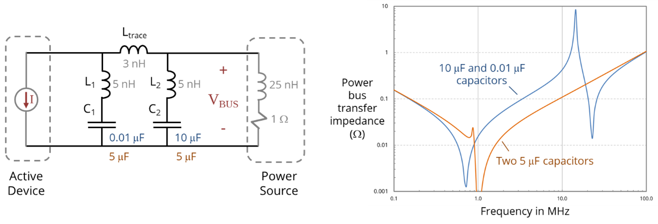
If more than one local decoupling capacitor is employed, they should have similar nominal capacitance values. The orange curve in the figure above shows the transfer impedance for the same circuit when the two capacitors both have a nominal value of 5 μF. In this case, their self-resonances are at nearly the same frequency, and the parallel resonance between them is significantly damped.
Note that below about 300 kHz, the transfer impedances of both circuits in the figure above are the same. At low frequencies, the total value of the connected capacitance determines the response. Above 50 MHz, both circuits exhibit the same transfer impedance. At high frequencies (above the self-resonant frequency of both capacitors), the connection inductance dominates, and the nominal capacitance values are no longer relevant.
Decoupling PCBs with Closely-Spaced Power/Power-Return Planes
There is a limit to how low the connection inductance can be when power is distributed to components on traces (generally several nanohenries or more). Many of the active devices found on circuit boards today can draw amperes of current at relatively high frequencies. These devices require very low power bus impedances that can only be achieved by distributing the power on closely spaced circuit board planes. Closely-spaced planes not only permit low-inductance connections; they also provide their own inter-plane capacitance, which can provide excellent decoupling at very high frequencies.
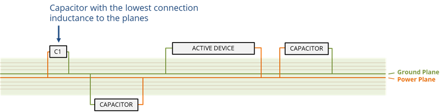
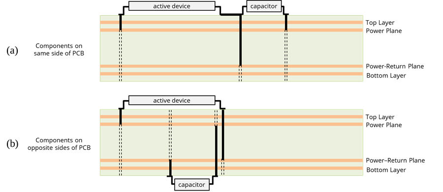
The figure below illustrates the cross-section of a board with power planes containing an active device and three decoupling capacitors. Note that for any given connection between the active device and a capacitor, the loop area between the planes is small relative to the area associated with the connections to the planes. Also, the planes are wide relative to the connecting via diameters, so the magnetic flux wrapping the planes is weak. The value of the connection inductance is dominated by the connection between the active device and the planes and the connections between the capacitors and the planes. In this example, the capacitor on the far left is connected through vias that are near each other and has the lowest connection inductance to the planes. This capacitor will provide more decoupling current to the active device than the other capacitors even though it is located farther away.
A lumped-element model for the power distribution impedance on a board with closely-spaced power and ground planes is shown below. If the planes are very close (e.g., less than 0.5 mm), the plane inductance is negligible. And at frequencies where the maximum dimensions of the board are much less than a wavelength, the plane impedance can be modeled with a single capacitor. Capacitors mounted on the surface of the board have a connection inductance as indicated in the figure. While this model is only valid at frequencies well below the first plane resonance, we will see that it generally serves as an excellent model at all frequencies where the decoupling capacitors are effective [3] [4].
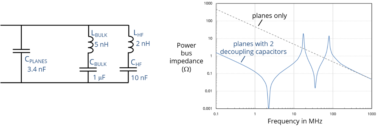
The circuit above models two capacitors connected to a pair of closely spaced planes. One of them, CBULK, is a large capacitor with a high nominal value intended to provide the capacitance needed for low-frequency decoupling. The other, CHF, has a small package size intended to facilitate the low-inductance connection to the planes needed for high-frequency decoupling.
At low frequencies, the inductances can be neglected, and the impedance of the power bus is approximately equal to,
All the capacitors on the board help to decouple the power bus, although the larger-valued capacitors are the most effective. At higher frequencies, the larger inductances become important. For example, the bulk capacitor represented in the circuit above resonates with its own connection inductance at,
The power bus impedance is very low near the self-resonant frequency, but above that, the bulk capacitor becomes an inductance, and impedance rises with increasing frequency. Eventually, the inductance of the bulk capacitor exhibits a parallel resonance with the remaining capacitors. At this parallel resonance, the impedance of the power bus peaks. As the frequency continues to increase, the smaller-valued capacitor with smaller connection inductance eventually goes self-resonant, producing another null in the power bus impedance. But that null will be followed by another peak when both capacitors look like inductors and form a parallel resonance with the plane capacitance. At the parallel resonant peaks, the impedance of the power bus can be very high, and the board will tend to ring at these frequencies if there is not sufficient loss to dampen these resonances.
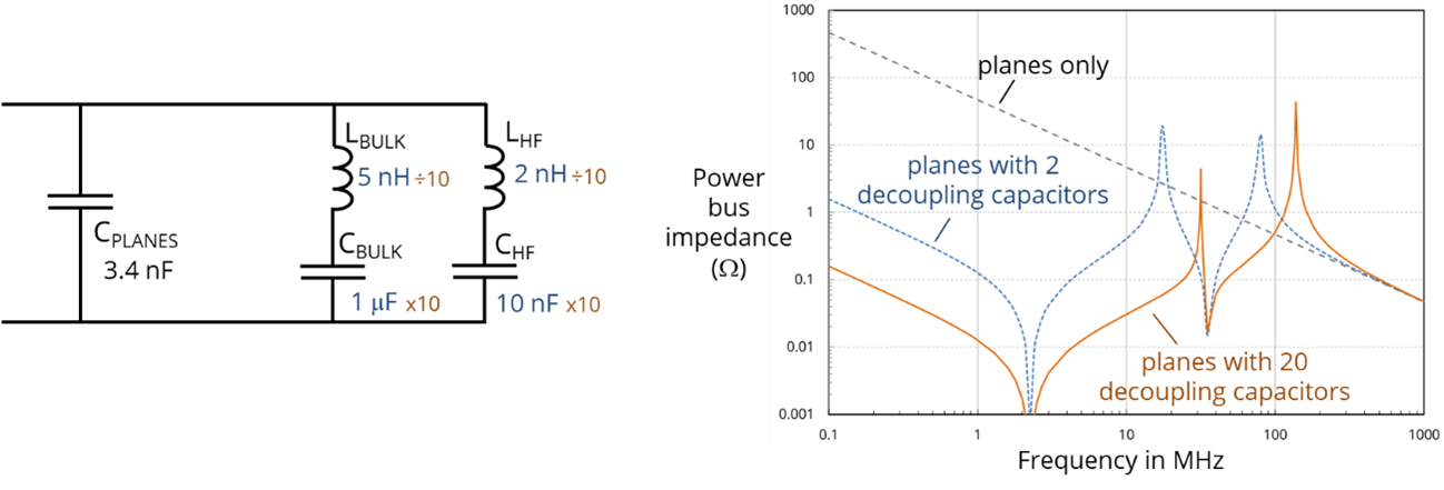
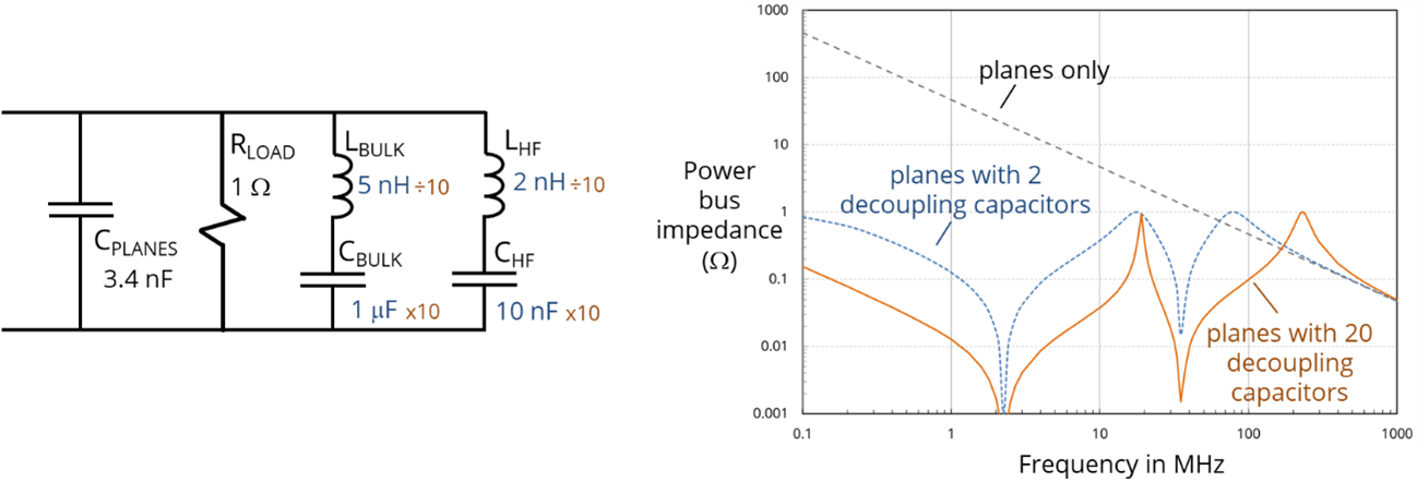
The decoupling bandwidth can be improved by adding more capacitors. Two identical capacitors in parallel have twice the capacitance and half the inductance of one capacitor. Ten times the number of capacitors will have ten times the capacitance and one-tenth of the inductance. The impact of increasing the number of decoupling capacitors is illustrated below. With 20 decoupling capacitors instead of 2, the impedance is reduced, and the frequency range over which the capacitors are effective is extended.
The peaks in the response shown above can be a concern for boards with relatively few components. Current is not easily drawn from the power bus at these frequencies, and a transient current draw could cause the bus voltage to oscillate. One way of preventing this is to choose capacitors with a range of values, so that their series resonances are spread across the entire frequency range of interest. For example, instead of using 10 high-frequency decoupling capacitors with a value of 10 nF, use 1 nF, 2 nF, 4.7 nF, 6.8 nF, 10 nF, 20 nF, 47 nF, 68 nF, 100 nF and 200 nF. This spaces the nulls in the response roughly equally across the log-frequency spectrum. The peaks occur between the nulls, so they are also spread out. Both the nulls and the peaks are more damped with this arrangement.
While spacing these resonances can be effective, it is not usually necessary or desirable if the board is heavily populated. The resistances in the power distribution due to the power draw of the active devices, the ESR of the decoupling capacitors, and other naturally occurring losses tend to provide enough damping so that these power bus resonances are not a significant concern. For example, the figure below shows the power bus impedance of the circuits above when the active devices provide 1 Ω of loading on the power bus. This could be the case, for example, if a 3.3-volt board drew 3.3 amps of DC current.
Power Plane Resonances
Note that, for the example above, the decoupling capacitors provided no benefit at frequencies above 200 MHz. When boards have closely spaced power and ground planes, the plane capacitance becomes a good source of high-frequency current. Surface-mounted decoupling capacitors with 1-2 nH of connection inductance are unable to provide enough current to compete with the planes at hundreds of megahertz. Because of this, simple circuit models that neglect the plane inductance work well over the entire range of frequencies where the surface-mounted decoupling capacitors are effective.
At higher frequencies, where the maximum dimensions of the plane pair are not small relative to a wavelength, the power planes can no longer be modeled as a simple capacitance. Planes with large surface areas and few connected components can behave like cavity resonators. At their resonant frequencies, they can radiate like patch antennas.
For rectangular planes, the first cavity resonance occurs when the largest dimension of the plane pair is a half wavelength (in the cavity dielectric). Various online calculators, such as the one here, can be used to determine the frequencies associated with higher-order modes. There are also numerical modeling tools available that can calculate the resonances associated with plane pairs of arbitrary shape.
If the power plane pairs are very closely spaced (e.g., less than 0.1 mm apart), the copper loss in the planes damps the resonances significantly. Similarly, if the planes are not so closely spaced but have a high density of attached components, the component losses damp the resonances. Because of this, power plane resonances are rarely a significant issue on heavily populated circuit boards. On the other hand, plane resonances should be anticipated when large areas of the plane pair extend into unpopulated regions of the board.
Decoupling PCBs with Widely Spaced Power Planes
Often, printed circuit boards will have solid power and ground planes, but the spacing between these planes will be 1 mm or greater. For these boards, the inductance associated with the planes can no longer be neglected, and the models for closely spaced planes do not apply. The plane inductance inhibits the ability of the planes to provide charge quickly. On the other hand, by careful placement of the decoupling capacitors, this inductance can be used to help pull current from the decoupling capacitors while reducing the power bus noise on the planes.
The figure below illustrates how this works. In this example, an active device and a decoupling capacitor are located on the top side of the board. The inductance between the planes is dominated by the magnetic flux that wraps the vias connected to the lower plane (in this case, the power plane). The flux wrapping each via adds in the region between the two vias. However, the flux wrapping the vias cancels outside this region. The flux between the vias represents an inductance that impedes the ability of the decoupling capacitor to supply current. The flux outside this region represents a mutual inductance that helps to pull charge from the decoupling capacitor [5], [6], [7].
If the via from the active device is located near the via from the decoupling capacitor, the mutual inductance is stronger. If the mutual inductance due to the loop area between the planes is greater than the self-inductance associated with the loop formed by the decoupling capacitor connection outside the planes, then more charge will be pulled from the decoupling capacitor than from the planes.
For widely spaced planes, when the two vias are very close to each other, the flux cancellation between the planes is high. This mutual inductance tends to force current to be drawn from the capacitor instead of the planes. This is exactly what we want if the goal is to keep noise currents off the planes.
When the active device and the local decoupling capacitor are on the same side of the board, the mutual inductance is maximized by sharing a via connection to the most distant plane, as illustrated in the upper figure below. On the other hand, if the decoupling capacitor and active device are on opposite sides of the board, the vias pulling current between the planes are not connected to the same plane. This case is illustrated in the lower figure below, where the capacitor’s power via needs to be located near the active devices' power-return (or GND) via.
If the mutual inductance between the planes is greater than the capacitor’s connection inductance above the planes, most of the current supplied to the active device will be pulled from the capacitor. When implemented correctly, this type of connection maximizes the current available to the active device and minimizes the voltage induced in the power planes.
Connecting Capacitors to Boards with Power Planes
It's important to note that the guidelines for placing decoupling capacitors on boards with widely spaced power planes are very different than the guidelines for boards with closely spaced power planes. When the planes are closely spaced, ALL the decoupling capacitors are global. All the decoupling capacitors respond when they see the voltage in the planes change. Each decoupling capacitor supplies a maximum current that depends entirely on the inductance of its connection to the planes. For closely spaced planes, the location of the decoupling capacitor is relatively unimportant. The connection inductance is the most important factor affecting the capacitor's ability to respond quickly.
For widely spaced planes, the capacitor sharing a via connection to the most distant plane provides most of the high-frequency current. The local capacitor responds even before the voltage in the planes drops. A well-mounted local decoupling capacitor provides nearly all the high-frequency current drawn by the nearby power pin. All of the other capacitors on the board can only respond when they see the voltage in the planes drop. It's important for the local decoupling capacitor to have a connection inductance that is lower than the mutual inductance between the planes. However, unlike capacitors with closely spaced planes, the ability of the capacitor to keep noise off the planes is not inversely proportional to this inductance. The connection needs to be "good enough," but further reductions in the connection inductance do not yield further reductions in the plane noise.
Whether the planes are closely-spaced or widely-spaced, the connection inductance between the high-frequency decoupling capacitors and the nearest power plane needs to be on the order of 1-3 nH. The main parameter determining the connection inductance is the loop area illustrated in the top half of the figure below. This area is bounded by the path of the current coming out of the planes, flowing through the capacitor, and back to the planes.

The distance from the power planes to the capacitor is a critical factor in determining this loop area. However, the distance between the connecting vias is equally important. Viewed from above, the power and power-return vias must be located as close to each other as possible. Typically, this means choosing an SMT capacitor with the smallest possible package size and locating the connecting vias in or adjacent to the mounting pads as indicated in the bottom right side of the figure above.
Note that vias located at opposite ends of the pads can have twice the distance between them as vias located to the side of the pads. This results in approximately twice the inductance, and, for global decoupling capacitors, twice as many capacitors would be required to achieve the same high-frequency performance.
In most situations, small SMT capacitors (e.g., 0402) with vias in or to the side of the pads represent the most cost-effective and space-effective decoupling. In certain situations, particularly when the plane area is very limited, the use of special low-inductance decoupling capacitor packages may be warranted. Low-inductance package options include reverse-aspect-ratio capacitors (e.g., 0204) that are wider than they are long. These capacitors allow two via connections to each pad and minimize the distance between power and power-return vias. Another option is capacitors that have four or more terminals that facilitate interspersed power and power-return connections.
References
[1] C. R. Paul, "Effectiveness of Multiple Decoupling Capacitors," IEEE Trans. on Electromagnetic Compatibility, vol. 34, no. 2, May 1992, pp. 130-133.
[2] T. Zeeff, T. Hubing, T. Van Doren and D. Pommerenke, "Analysis of Simple Two-Capacitor Low-Pass Filters," IEEE Trans. on Electromagnetic Compatibility, vol. 45, no. 4, Nov. 2003.
[3] T. H. Hubing, J. L. Drewniak, T. P. Van Doren, and D. Hockanson, "Power bus decoupling on multilayer printed circuit boards," IEEE Trans. on Electromagnetic Compatibility, vol. 37, no. 2, May 1995, pp. 155-166.
[4] M. Xu, T. Hubing, J. Chen, T. Van Doren, J. Drewniak and R. DuBroff, “Power-bus decoupling with embedded capacitance in printed circuit board design,” IEEE Trans. on Electromagnetic Compatibility, vol. 45, no. 1, Feb. 2003, pp. 22-30.
[5] T. H. Hubing, T. P. Van Doren, F. Sha, J. L. Drewniak, and M. Wilhelm, "An Experimental Investigation of 4-Layer Printed Circuit Board Decoupling," Proceedings of the 1995 IEEE International Symposium on Electromagnetic Compatibility, Atlanta, GA, August 1995, pp. 308-312.
[6] J. Fan, J. Drewniak, J. Knighten, N. Smith, A. Orlandi, T. Van Doren, T. Hubing and R. DuBroff, "Quantifying SMT Decoupling Capacitor Placement in DC Power-Bus Design for Multilayer PCBs," IEEE Trans. on Electromagnetic Compatibility, vol. EMC-43, no. 4, November 2001, pp. 588-599.
[7] J. Fan, W. Cui, J. Drewniak, T. Van Doren, J. Knighten, "Estimating the Noise Mitigation Effect of Local Decoupling in Printed Circuit Boards," IEEE Trans. on Advanced Packaging, vol. 25, no. 2, May 2002, pp. 154-165.