Some of the Worst EMC Design Guidelines
These guidelines tend to cause more EMC problems than they prevent.
Circuit Board Layout
Circuits on a printed circuit board should be grouped by type, with power circuits closest to the connector and high-speed digital circuits farthest from the connector.
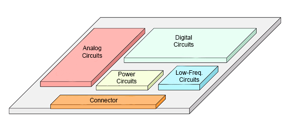
This design guideline (or variants that indicate other groupings) is probably responsible for more crazy board layouts than any other individual EMC design guideline. It ignores the fundamental idea that different boards have different functions. We have seen boards with very high-speed digital signals routed all the way across the board in an attempt to keep the digital components away from the connector.
It is certainly important to consider the function and speed of components when deciding where to place them. However, any general statements about placement relative to the connector are more likely to produce a bad design than a good one. Usually, but not always, it's a good idea to put the components that send or receive signals through the connector nearest the connector. Placement is important, but design guidelines that dictate placement without considering the function and signals associated with the circuits are very dangerous.
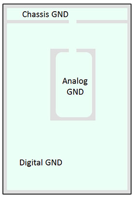
Solid ground planes should be gapped between analog and digital circuits.
This is probably a close second in the competition for the worst EMC design guideline ever conceived. There are some (very few) situations where gapping a ground plane between analog and digital circuits is a good idea. These situations are always related to a need to keep low-frequency (< 100 kHz) currents produced by a noisy circuit from sharing the same copper return path as currents in a circuit that is sensitive to currents approximately 3 orders of magnitude lower. Unfortunately, gapping a solid ground plane can cause enormous problems by interfering with the flow of high-frequency currents and generating voltages that ultimately result in radiated emission problems. In many cases, leaving the plane solid and letting both circuits share the plane is fine. In situations where low-frequency isolation is required, it is almost always better to provide separate return paths for these circuits. This is generally accomplished using a trace or plane on a different board layer.
The ground plane under the I/O (connectors) should be separated from the digital ground plane with one connection point between them.
 This guideline was not unreasonable 30 years ago when most boards had two layers, were less densely populated, and operated at relatively slow speeds. However, today, this is generally one of the worst possible ways to lay out a ground plane. Generally, the goal should be to achieve a low-impedance connection between chassis and digital ground at radiated emissions frequencies (e.g., above 30 MHz) and control the flow of any low-frequency (e.g., <100 kHz) currents by isolating the chassis from the digital ground at low frequencies. This layout accomplishes the opposite of that. As a result, products employing this design usually have lots of capacitors bridging the gap between the digital and chassis grounds. This effectively forms a notch filter of questionable value.
Low-frequency isolation and high-frequency bonding are much better achieved by putting the chassis ground on a separate layer and overlapping it with the digital ground. This allows a good high-frequency connection to be made between them using multiple low-inductance SMT capacitor connections. A low-frequency connection can be made between digital ground and chassis ground at the single point where it makes the most sense, which may or may not be in the vicinity of the I/O.
The general rule-of-thumb that a solid ground plane should never be split applies here. If the ground plane needs to be cleared out of a particular area (e.g., under magnetics, power inverters, or for high-voltage isolation), that is often fine. Splitting/gapping a ground plane, however, is almost always a bad idea.
Single-point grounds should be used for low-frequency circuits. Multi-point grounds should be used for high-frequency circuits.
While the underlying sentiment of this guideline is not necessarily incorrect, system designers who do not understand the difference between "ground" and "current return" use this guideline to justify some terrible designs. At low frequencies, we do not want all return currents to flow through a single point. Yet that is precisely what happens when people mindlessly try to apply this concept. Generally speaking, we want to control the flow of low-frequency currents by limiting the options. We control the flow of high-frequency currents by providing one good option. The concept of single-point and multi-point grounds is rarely helpful and often a significant source of bad design ideas.
Provide a digital-ground-to-chassis connection at the clock/oscillator location.
More often than not, this is a bad idea. If your design is attempting to keep chassis currents off of the digital ground plane by employing a single-point connection, then that connection should be along the edge where the I/O connectors are located. Normally, clocks and oscillators are kept out of this area, so making a connection near the clock/oscillator would destroy the single-point nature of the ground. Even if no attempt is being made to control low-frequency currents, there is generally no good reason to try to make a digital-ground-to-chassis ground connection near a clock/oscillator.
All traces longer than one-quarter wavelength at the highest frequency of interest should be terminated with a matched resistance.
This doesn't sound like a controversial design guideline, but it causes many designers to do exactly the wrong thing in many situations. Generally speaking, it is better to relate the propagation delay of the trace to the risetime of the signal. If the propagation delay is greater than the risetime, we might need to think about a matched termination. (Note that "highest frequency of interest" is poorly defined, whereas propagation delay and risetime are easily determined.) However, our first impulse should not be to match the trace. The best solution is to slow the risetime. Matched terminations actually make risetimes faster, and they pull more current from the source. Unless you're building very high-speed digital boards or very large boards, few (if any) traces should require a matched termination.
These infamous design guidelines have become "urban legends" in the EMC world.
Circuit Board Layout
Traces should not make sharp right-angle turns.
Nobody seems to know for sure where this guideline originated. EMC engineers often say it's a manufacturing issue. Board manufacturers say it's an EMC issue. Chamfering the corner on a wide, impedance-controlled trace may be a good idea at Gbps data rates. However, there is generally no advantage to making two 45-degree turns as opposed to making one 90-degree turn.
Power plane edges should not be flush with the edges of ground planes. They should be pulled in by a distance of 20 times the spacing between the planes (a.k.a., the 20-H Rule).
While it is possible to conceive of situations where making the power planes slightly smaller than the ground planes might be a good idea (e.g., to prevent coupling of power bus noise to cables draped over the edge of a board), it is rarely necessary to do this. Making the power plane smaller than the ground plane does not reduce the radiation from the planes unless the power plane is sandwiched between two ground planes. Power planes sandwiched between two ground planes are not likely to be a radiated EMI problem, even if the power planes are the same size as the ground planes. If there is a desire to reduce the fringing field at the edge of the board, 2-H or 3-H is generally more than adequate.