EMC Question of the Week: December 8, 2025
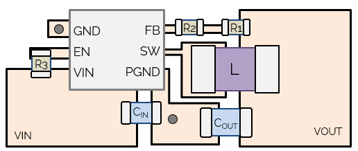
The datasheet for a DC-to-DC power converter (12 V to 3.3 V) switching at 1 MHz recommends the layout shown in the figure. All components are on Layer 1. Layer 2 is a solid return (GND) plane. Which of the following components needs to be relocated?
- CIN
- COUT
- R2
- All of the above
Answer
The best answer is “d.” The datasheet layout has several problems. Perhaps the most egregious is that CIN and COUT share a connection to the GND plane. This couples the switching currents from the input of the buck converter directly to the output. A converter switching at 1 MHz or higher should never have an isolated PGND. CIN should be located near the VIN pin of the converter and connected to the GND plane with a dedicated via in or adjacent to its solder pad. COUT should be located near the VOUT side of the inductor. It should also have a dedicated via to GND in or adjacent to its solder pad. Both capacitors should be kept away from the switching trace between the converter and the inductor. R2 should also be kept away from the switching trace to keep switching noise from coupling into the feedback signal.
Have a comment or question regarding this solution? We'd like to hear from you. Email us at