EMC Question of the Week: November 18, 2024

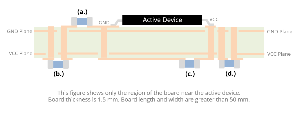
An active device is mounted on a 4-layer board with a GND plane on Layer 2 and a VCC plane on Layer 3. The spacing between Layers 2 and 3 is 1 mm. Which of the four decoupling capacitors depicted in the figure provides the best high-frequency decoupling?
- (a.)
- (b.)
- (c.)
- (d.)
Answer
The best answer is “d.” The capacitors at locations (a.) and (c.) are connected through too much inductance (loop area) to be helpful at the highest frequencies. The capacitor in location (d.) takes advantage of the mutual inductance between its GND via and the active device's VCC via to provide the best high-frequency decoupling. It is the only decoupling capacitor in the figure that provides high-frequency current before the voltage between the power planes drops. The remaining capacitors are global capacitors that provide charge in response to a drop in the plane voltage.
In this example, the (d.) capacitor could have been located on the top of the board allowing it to share the VCC via with the active device. This would have maximized the mutual inductance and is typically the preferred method for providing local high-frequency decoupling on boards with widely spaced power distribution planes.
Note that the goal of printed circuit board decoupling at high frequencies is generally to minimize the connection inductance between the decoupling capacitors and the active device power inputs. And while that is almost always the goal, the best method for achieving that goal can depend greatly on the geometry of the power distribution conductors and the board's layer stack-up.
Have a comment or question regarding this solution? We'd like to hear from you. Email us at
