EMC Question of the Week: December 11, 2023
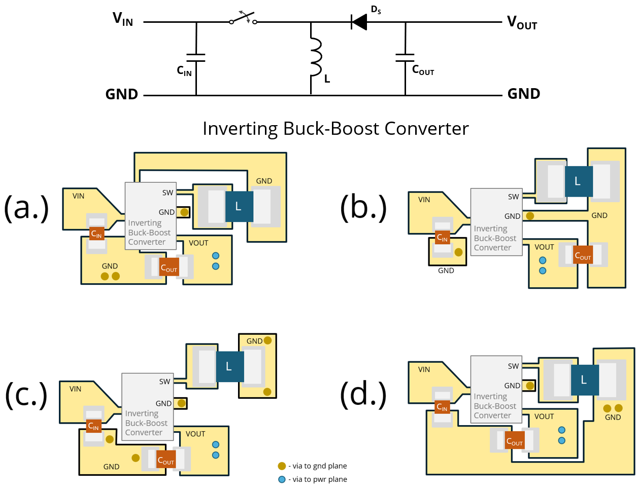
The input to a 1-MHz inverting buck-boost converter is +5 V and the output is -3.3 V. Which of the board layouts shown here is least likely to exhibit unacceptable conducted or radiated emissions if layer 2 is a solid GND plane?
Answer
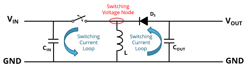
The best answer is “c.” As with most DC-to-DC converter layouts, it's important to minimize the electric-field coupling from the switching voltage node and the magnetic-field coupling from the switching current loop. Both layouts (a.) and (d.) bring the switching voltage node (SW) very close to VOUT. Switching noise can couple to VOUT and be carried to other parts of the board.
Option (b.) does a good job of isolating the switching voltage node, but the switching current loop is much larger than it needs to be. The current path from the converter at VIN through CIN to GND, then through COUT to VOUT and back to the converter forms a large loop that couples switching noise to both VIN and VOUT.
Option (c.) does a pretty good job of minimizing the area of the switching current loop while also isolating the switching voltage node. Of the four choices presented, it is the best one.
Have a comment or question regarding this solution? We'd like to hear from you. Email us at