EMC Question of the Week: October 16, 2023
The figure below shows four DC-to-DC step-up converter layouts. In each case, the traces shown are on the top layer, and the layer below is a solid ground plane. If the input voltage comes from a source off the board, which of these layouts is best for containing conducted and radiated emissions? 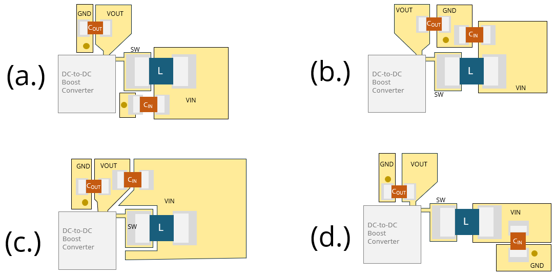
Answer
The best answer is (d.). To contain the switching noise, it is important to minimize the E-field coupling from the switching voltage node and the H-field coupling from the switching current loop. For a boost converter, the switching current loop is the connection from the switches to the output capacitor.
In Circuit (a.), noise from the switching node E-field couples to VIN and CIN, which carries the noise back to the power input.
In Circuit (b.), COUT and CIN share the same connection to the ground plane. This causes H-field coupling of noise from the switching current loop to VIN. This circuit reflects the layout advice in many old datasheets and application notes. This outdated advice stems from a time when switching frequencies were in the kilohertz and common-impedance coupling was more of a problem than magnetic-field coupling. Today, layouts like this that magnetically couple noise from the switching current loop to other circuits are a common source of conducted and radiated emissions.
In Circuit (c.), CIN connects to VOUT instead of GND, and VIN comes too close to the switching node.
In Circuit (d.), the switching loop area is minimized and kept far from other circuits that might carry the noise away from the area. Also, the switch node is small and relatively isolated minimizing E-field coupling to other circuits that could carry the noise away.
Note that the switching currents flow out of the converter on VOUT, through COUT to the ground plane on layer2. They return to the converter by flowing on layer 2 underneath the body of the COUT capacitor. Therefore, it doesn't matter that the via connection to the ground plane is not between COUT and the converter. The loop area is approximately the same either way.
One thing that all four layouts do correctly is keeping the switching currents above the ground plane. Pulling the switching currents through the board (e.g., by locating COUT on the backside) can be an effective way to couple switching noise to other circuits on the board.
Note: This week's question is very similar to last week's question, but the converters step the voltage up instead of stepping the voltage down. The layout options are also very similar with the locations of VIN and VOUT swapped.
Have a comment or question regarding this solution? We'd like to hear from you. Email us at