EMC Question of the Week: March 27, 2023
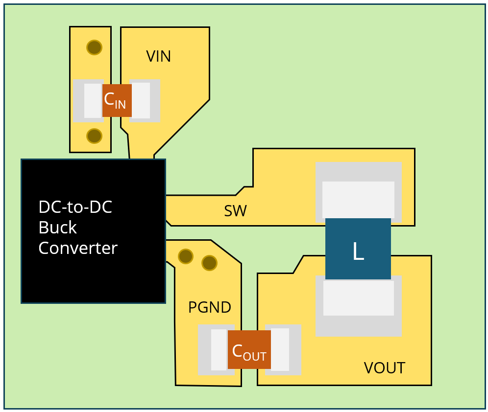
The 1-MHz buck converter layout in this figure is poorly done. Layer 2 is a solid GND plane. Cin connects to GND. Cout connects to PGND. Every ground pin of the converter IC connects to both PGND and GND. Which component is grounded incorrectly?
- CIN
- COUT
- the converter IC
- the inductor
Answer
The best answer is “b.” COUT should never share an isolated ground with CIN or any other component. In fact, this layout shouldn't even have a PGND. Currents at MHz frequencies and higher take the lowest inductance path and don't need isolated returns to prevent them from spreading uncontrollably. In a buck converter layout, CIN and COUT should both connect directly to the GND plane on Layer 2.
Another problem with this layout is that the switch-node (SW) is larger than it needs to be. The surface area of the switch-node should always be minimized and kept away from other traces or components that could carry the switching noise away from that part of the board. A better converter layout is shown below.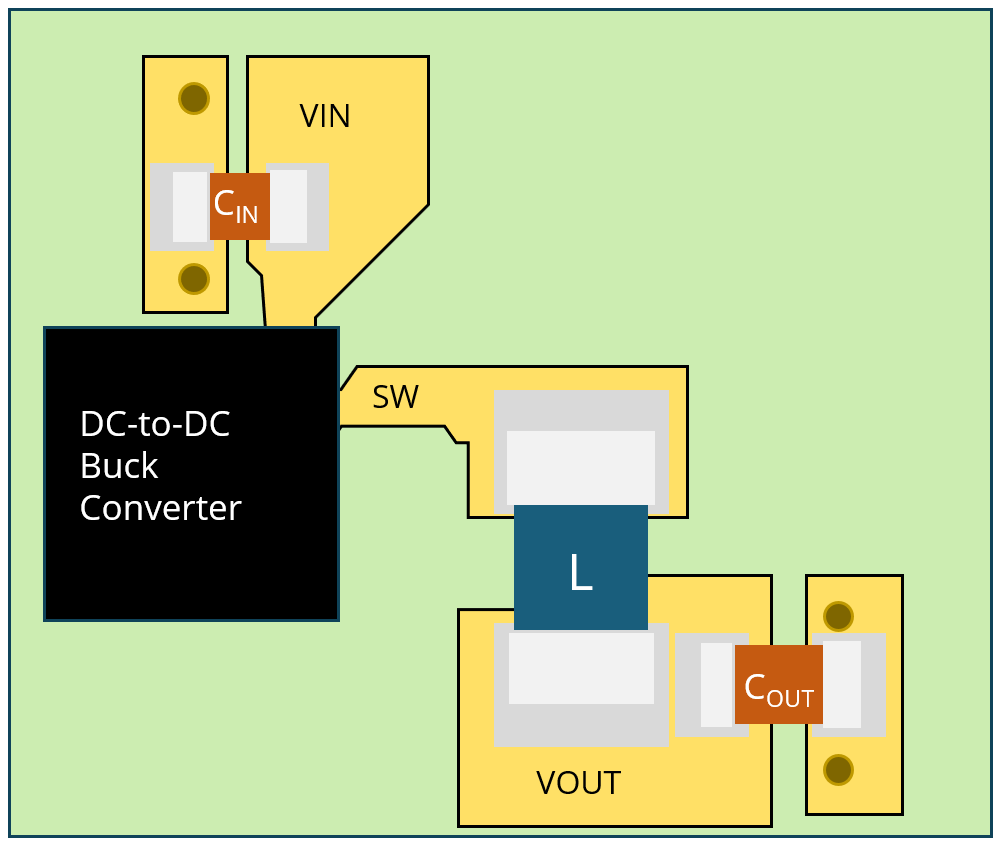
Have a comment or question regarding this solution? We'd like to hear from you. Email us at