EMC Question of the Week: February 7, 2022
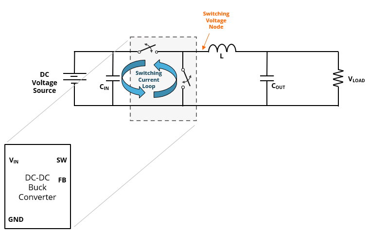
A 2-MHz synchronous buck converter is used to convert 12 VDC to 3.3 VDC. The high-side and low-side switches are internal to the converter IC. The inductor is external. The current with the highest time rate of change (dI/dt) flows through which external component?
- input capacitor
- output capacitor
- snubber capacitor
- inductor
Answer
The correct answer is “a.” The high dI/dt switching current loop in a synchronous buck converter flows through the high- and low-side switches and the input capacitor. For that reason, it's very important to minimize the loop area of the connection between the input capacitor and the converter IC. Other nets (other than GND) should be kept away from this current loop to avoid magnetic field coupling that could carry the switching noise to other parts of the circuit board.
It's also important to minimize the surface area of the switching voltage node, which connects the IC to the inductor. This node should be kept away from other nets (other than GND) to avoid electric field coupling that could carry the switching noise to other parts of the circuit board.
Note: The current with the highest time rate of change never flows through a properly configured inductor. Inductors limit the time rate of change of the current. Also, a 12-volt converter switching at 2-MHz does not require or benefit from a snubber capacitor.
Have a comment or question regarding this solution? We'd like to hear from you. Email us at