EMC Question of the Week: November 29, 2021
In a multi-layer printed circuit board, a via that connects a trace on an outer layer to traces on one or more inner layers, but does not pass all the way through the board, is called a
- blind via
- buried via
- stubby via
- via stub
Answer
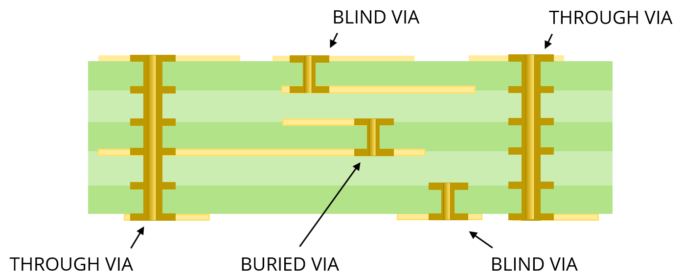
The correct answer is “a.” A blind via connects copper on an outer layer to copper on one or more inner layers without passing all the way through the board. Buried vias connect copper on two or more inner layers without connecting to either outer layer. Blind and buried vias enable boards to be laid-out with a higher density of signal traces. However, they generally require additional lamination steps, which can increase the manufacturing cost of the circuit board.
A via stub refers to the unused portion of a through via. For example, if a through via is used to connect traces on Layers 1 and 2 of a six-layer board, the portion of the via extending through Layers 3 to 6 is a via stub. Via stubs can introduce an unwelcome lumped capacitance in boards carrying very high-speed signals. In some cases, via stubs are removed by back drilling after the final plating step.
Have a comment or question regarding this solution? We'd like to hear from you. Email us at