EMC Question of the Week: July 13, 2020
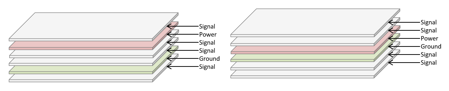
The best layer stack-up for a 6-layer printed circuit board is,
- S-S-P-G-S-S
- S-G-S-S-P-S
- SP-G-S-S-G-S
- none of the above
Answer
The best answer is "d". The truth is there is no guideline for the optimum layer stack-up that applies to more than a small subset of all boards. Optimum layer assignments depend on many factors. Any attempt to determine layer assignments based on a general guideline is unlikely to produce an optimum design.
The first option, with power and ground on layers 3 and 4 is useful in situations where it is necessary to have solid power and ground planes on adjacent layers. An example of this might be an automotive or industrial sensor that has large high-speed ICs requiring low-impedance power distribution even though the data rates external to the ICs are relatively slow. The second option may be useful when the power requirements of the ICs are less demanding, but there is a need to shield some of the signal traces. The third option, where power is routed on traces rather than planes, may be optimum when none of the ICs have more than one or two power pins, but there are a large number of high-speed signals.
Of course, there are dozens of permutations of the above stack-ups that may be preferable depending on the application. For example, S-G-P-S-G-S might be appropriate in situations where the power planes need to be both adjacent and very near to one surface. This stack-up sacrifices signal routing area for an extra ground plane.
S-S-SP-G-S-S might be optimum in boards with lots of low-speed connections. This stack-up doesn't provide a nearby return plane for all signals, but it might be a better alternative than an eight-layer board for some applications.
Have a comment or question regarding this solution? We'd like to hear from you. Email us at