EMC Question of the Week: June 8, 2020
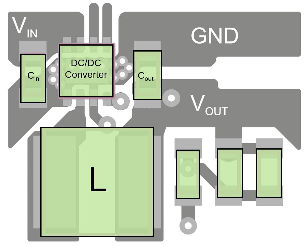
For the DC/DC buck converter shown in the figure, the high-frequency switching current loop is the trace and pads connecting the converter IC to
- Cin
- Cout
- L
- GND
Answer
The correct answer is "a". The high-frequency switching current loop (i.e. the current path with the uncontrolled dI/dt) is the connection between the converter IC and the input capacitor. This is always the case for buck topologies used for step-down DC-to-DC converters. The area of this loop should always be minimized and it should be kept far from traces or circuits that could carry the coupled switching noise away from the converter.
The layout shown is based on a figure in a Texas Instruments (TLV62065) data sheet. This layout does good job of minimizing the area of the switching current loop. The layout assumes there is a solid GND plane layer directly below the converter components. This is an essential part of the layout as it minimizes the inductance of the loop in the figure.
Note that it was not essential to have GND on the top layer for this layout. Cin could have simply connected to VIN next to the converter IC and to the GND plane on Layer 2 through vias on or in the other solder pad. Also note that the GND on the top layer next to Cout was not necessary. Cout should be connected directly to the GND plane on Layer 2 and should never share via connections to the GND plane with Cin.
Have a comment or question regarding this solution? We'd like to hear from you. Email us at