EMC Question of the Week: June 1, 2020
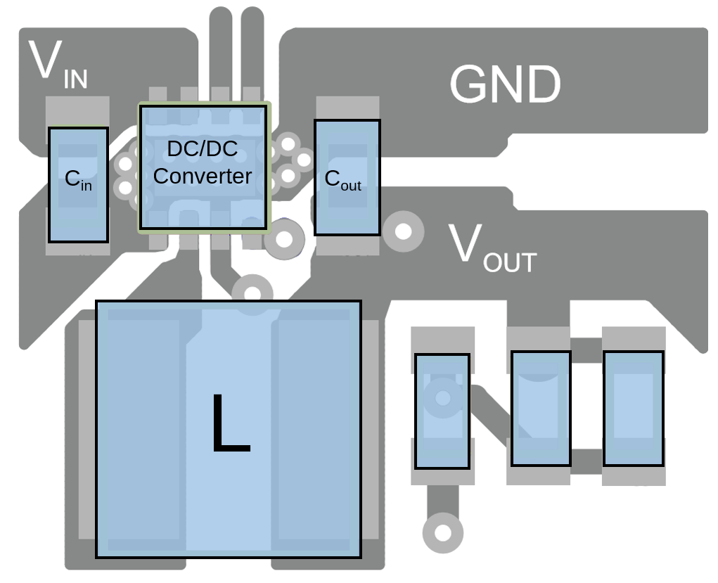
For the DC/DC buck converter shown in the figure, the switching voltage node is the trace and pads connecting the converter IC to
- Cin
- Cout
- L
- GND
Answer
The correct answer is "c". The switching voltage node (i.e. the node with the uncontrolled dV/dt) is the connection between the converter IC and the inductor. This is always the case for both buck and boost topologies. The area of this node should always be minimized and it should be kept far from traces or circuits that could carry the coupled switching noise away from the converter.
The layout shown is based on a figure in a Texas Instruments (TLV62065) data sheet. This layout does an excellent job of minimizing the area of the switching voltage node. The layout assumes there is a solid GND plane layer directly below the converter components.
Have a comment or question regarding this solution? We'd like to hear from you. Email us at