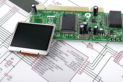
Printed Circuit Board Design for EMC and Signal Integrity
Next online open-enrollment offering: September 28 - October 8, 2026 • Registration Page
Description
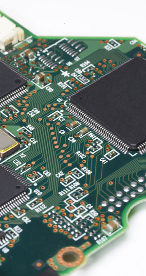
Today's rapid development cycles require products to meet their EMC requirements the first time they come into the lab for testing. Board layout changes and other EMC "fixes" can significantly add to the cost of a product and/or delay its development schedule. First-pass compliance with EMC requirements starts with the circuit board layout. Printed circuit board layout is often the single most important factor affecting the electromagnetic compatibility of electronic systems. Boards that are auto-routed or laid out according to a list of “design rules” do not usually meet electromagnetic compatibility requirements on the first pass, and the products using these boards are more likely to require expensive fixes such as ferrites on cables or shielded enclosures. Taking the time to ensure that components are properly placed, transition times are not left to chance, and traces are optimally routed will generally result in products that meet all electromagnetic compatibility and signal integrity requirements on time and on budget.
Recognizing poor design features early in a product’s development can save a lot of time and expense later on. This course stresses the fundamental concepts and tools that board designers must be familiar with to avoid electromagnetic compatibility and signal integrity problems. Students completing the course will be able to make good decisions regarding component selection, component placement, and trace routing. In addition, students will have the knowledge and tools necessary to design effective power distribution and grounding strategies for both digital and mixed-signal boards.
Continuing Education Credit: 1.2 CEUs, 12 PDHs
Course Outline
- Introduction
- Impact of Layout on Product Compliance and Cost
- Review of EMC Fundamentals
- The Design Review
- Current Return
- Concept of Least Impedance
- Following the Current
- Grounding
- Ground vs. Current Return
- Locating Ground on Your Board
- Identifying and Characterizing the Noise Sources
- Digital Signals as Sources of EMI
- Integrated Circuits as Sources of EMI
- Parasitic Oscillations
- Differential Mode to Common Mode Conversion
- Transmission Lines
- Transmission Line Physics
- Transmission Lines on Circuit Boards
- Crosstalk
- Common Impedance Coupling
- Electric Field Coupling
- Magnetic Field Coupling
- Coupling Between Matched Transmission Lines
- Strategies for Mixed-Signal PCB Layout
- Managing Current Return Paths
- Managing Ground
- Design Examples
- Filter Design and Layout
- Insertion Loss
- First-Order Filters
- Second-Order Low-Pass Filters
- Third-Order Low-Pass Filters
- Impact of Component Parasitics
- Circuit Board Shielding
- Shielding Principles
- How and When to Shield PCBs
- Terminating Cable Shields
- DC Power Distribution and Decoupling
- Effective Power Distribution Strategies
- Choosing and Locating Decoupling Capacitors
- Low-Inductance Capacitor Connections
- Isolating PLLs and Other Sensitive Devices
- Key Design Considerations for EMC Compliance
- Conducted Emissions Compliance
- Radiated Emissions
- Radiated Immunity
- Bulk Current Injection
- ESD and Transient Immunity
- An EMC Compliance Strategy
- Identify the EMC Ground
- identify the Antennas / Ports
- Identify the Sources / Victims
- Control Bandwidths
- Quantify Maximum Coupling
- Computer Modeling
- Circuit Solvers and Online Calculators
- Quasi-static and Full-Wave Field Solvers
- Design Rule Checkers
- Maximum Emissions / Coupling Calculators
- Specific Design Examples
- DC-to-DC Converter Layout
- Protecting Intentional Antennas
- Motor Drivers
- Audio Boards
- Others Provided by the Class
- Course Summary
- Review of Key Concepts
- Resources for EMC and Signal Integrity Engineers
Course Instructor

Dr. Todd H. Hubing is a Professor Emeritus of Electrical and Computer Engineering at Clemson University and former Director of the Clemson Vehicular Electronics Laboratory. He and his students at Clemson have worked on the development and analysis of a wide variety of electronic products. EMC design rules can vary greatly depending on whether you are designing high-speed computing equipment, low-cost mixed-signal consumer products, or high-power industrial controls, but the basic EMC principles are the same in all industries. By applying these principles in an organized manner, it is possible to review a design circuit-by-circuit to guarantee that any particular EMC requirement will be met. This approach is more effective than the blind application of design guidelines and is the primary emphasis of every EMC design class taught by Dr. Hubing.