Practical EM Shielding
Shielded enclosures generally surround a product’s circuitry on all sides. Care is taken to ensure that all apertures are small and every seam is sealed. On the other hand, it is not uncommon to find shields that don’t surround the entire product. Often, a shield partially covers only a few circuits. These shields may be penetrated by unfiltered wires and sometimes consist of a single plate of metal that may or may not be connected to ground.
Why are apertures and seams so important in some applications and completely irrelevant in others? The answer relates to the fact that there are different kinds of shielding for different applications. It is convenient to divide enclosure or component shields into 3 categories: electric-field shields, magnetic-field shields, and shielded enclosures. The best shielding strategy in any given application depends on a number of factors, including the electrical characteristics of the circuit or system being shielded, physical constraints (e.g., size, weight, and accessibility), and cost.
Electric-Field Shields
A perfectly conducting enclosure that completely surrounds a given volume prevents anything within that volume from electrically coupling to anything outside that volume. This type of enclosure is called a Faraday cage. Electric fields generated within the volume either terminate on objects within the enclosure or on the inner surface of the enclosure wall, as illustrated in Fig. 1(a). Free charge on the enclosure relocates itself as needed to cancel the fields within or external to the enclosure exactly.
Enclosures that are not perfectly conducting are still good Faraday cages as long as the charges can redistribute themselves fast enough to cancel the internal fields. Most metallic enclosures without significant seams or apertures provide excellent electric field shielding over a wide range of frequencies.
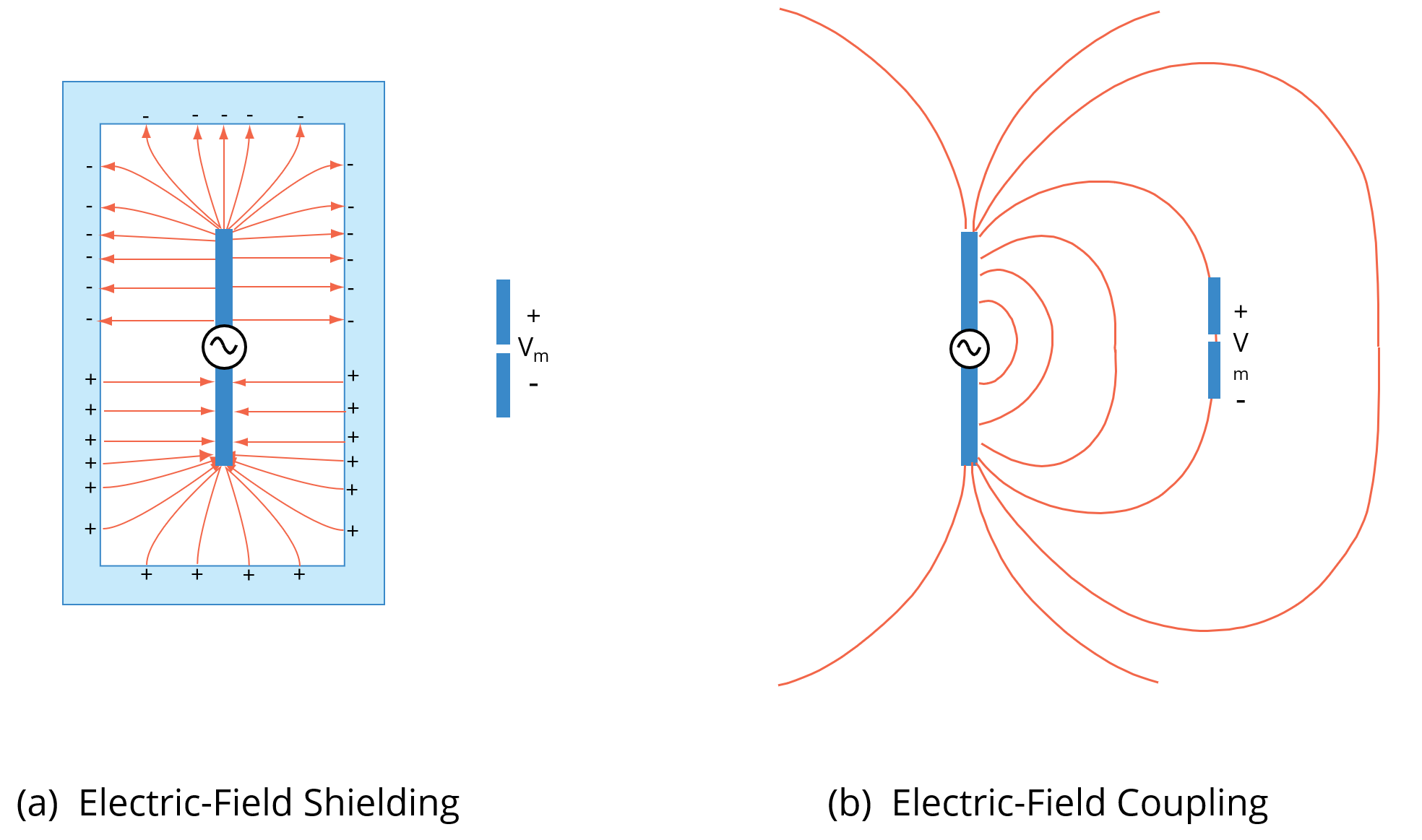
Fig. 1. Electric Field Coupling/Shielding.
Without the shield in Fig. 1(a), field lines may terminate on other conductors, resulting in potential differences between these conductors as indicated in Fig. 1(b). However, a partial shield [Fig. 2(a)] or even a simple metal plate [Fig. 2(b)] can substantially reduce these potentials by altering the path of the electric field lines and preventing the stronger field lines from reaching the victim circuit.
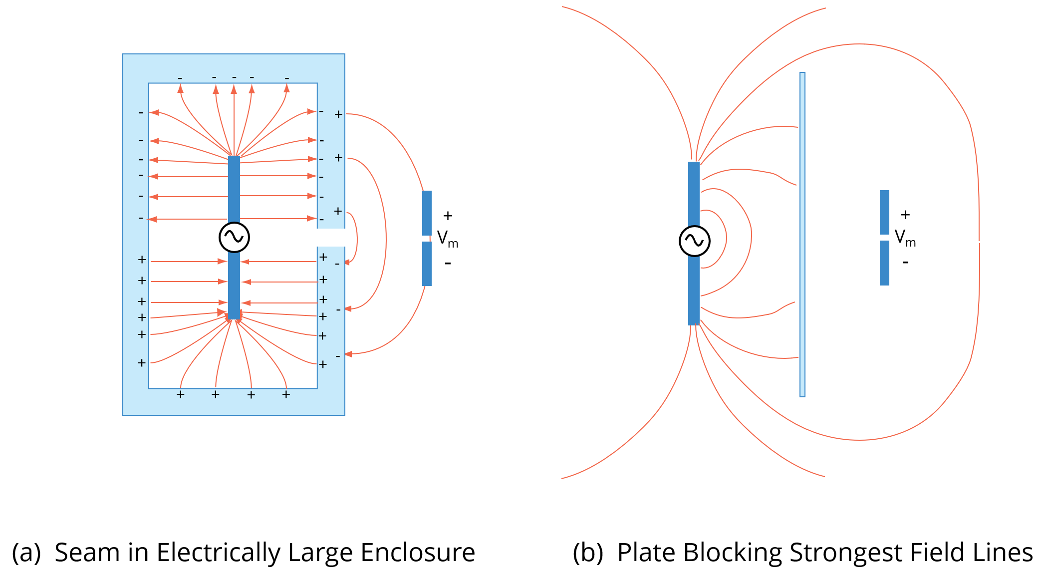
Fig. 2. Partial Electric Field Shields.
Key concepts for practical electric field shielding are choosing a location that will intercept the stronger field lines and choosing a suitably conductive shield material. How conductive must the material be? That depends on the frequency or time rate-of-change of the fields. As long as charges are able to move freely enough to reorient themselves as fast as the field changes, cancellation of the external fields will be achieved.
For static electric fields, almost any material will look like a conductor, since the free charge can slowly reposition itself. However, for high-frequency electric fields, the conductivity of the shield material must be high enough to allow the charge to move quickly back and forth.
Intercepting electric field lines with a conductive shield is primarily a matter of visualizing the field lines that are potentially responsible for the unwanted coupling and positioning the shield so that it blocks these fields. A few examples are provided in Fig. 3.

Fig. 3. Electric Field Shielding Examples.
Note that field lines terminating on a conductor imply there is a negative charge induced at that point. There is a positive charge at locations where field lines exit a conductor. If the field is time varying, there will be a current on the surface of the conductor as these charges move back and forth.
Magnetic-Field Shields
Because there are no free magnetic charges, it is not possible to terminate lines of magnetic flux on a shield. However, it is possible to redirect magnetic flux lines to prevent unwanted coupling. This can be accomplished by electric currents induced in an electrically conductive shield or by altering the path of magnetic flux lines using permeable (μr>>1) materials.
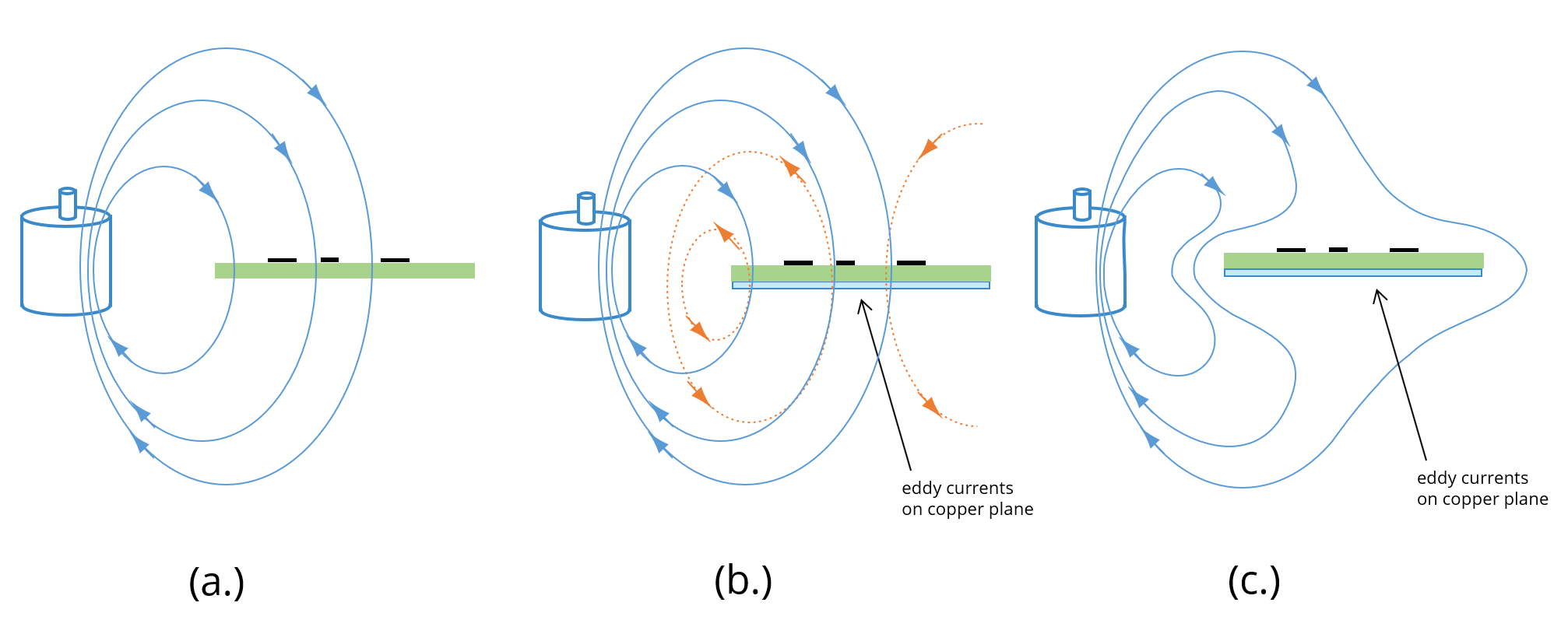
Fig. 4. Magnetic field shielding with good conductors.
Consider the configuration shown in Fig. 4(a). A vertical magnetic field from an electric motor couples to a small circuit board, resulting in interference. Fig. 4(b) shows the same configuration with an aluminum plate below the circuit. If we define any closed-loop path on the surface of the plate that is penetrated by the incident magnetic field, Faraday’s law tells us that an electric field must exist on the surface such that,
(1)
where the right-hand side of this equation is the time rate of change of the total magnetic flux coupling the loop. However, any electric field on the surface of a good conductor will cause currents to flow in that conductor. These currents will generate their own magnetic flux that opposes the incident flux. In a perfect conductor, the flux generated by these currents would perfectly cancel the incident flux, causing both sides of (1) to equal zero (i.e., no flux penetrating the conductor and no tangential electric field on the surface).
Currents induced in a conducting material by a time-varying magnetic field in this manner are called eddy currents. Both the incident field and the magnetic field created by the eddy currents are shown in Fig. 4(b). The sum of both fields is shown in Fig. 4(c). Note that the eddy currents cause the magnetic flux to be diverted around the plate and significantly reduce the coupling to the circuit.
In order to divert a magnetic field with a conductive plate, it is important to be able to develop sustained eddy currents. Since the eddy currents are driven by time-varying fields, a conductive plate cannot divert a static magnetic field. Even if the field is slowly varying, losses in the conducting plate will cause the eddy currents to dissipate, allowing the magnetic flux to penetrate the plate. For this reason, conductive materials are generally poor magnetic shields at low frequencies (e.g., below a few hundred kHz). Conductive magnetic shields are also ineffective if they have slots or gaps that interrupt the flow of the eddy currents.
At kHz frequencies or lower, it is generally necessary to use permeable (magnetic) materials (μr>>1) to divert magnetic fields. Since these materials have a reluctance much less than air, magnetic field lines can effectively be rerouted by providing an alternative path through a permeable material such as steel or mu-metal. Fig. 5 illustrates how a shield made from a permeable material can be used to protect the circuit in the previous example.
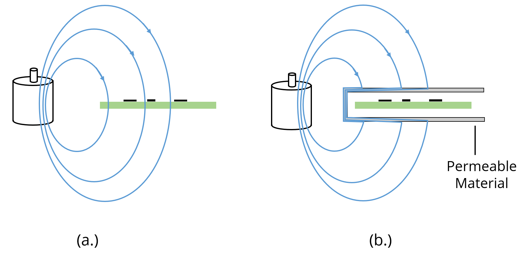
Fig. 5. Magnetic field shielding with magnetic materials.
Note that it is important for the magnetic material shield to divert the magnetic flux all the way around the object being shielded. A plate of magnetic material above or below the circuit board would provide no shielding at all.
Shielded Enclosures
At high frequencies, it is possible for the currents induced on the shield to radiate as well as (or possibly much better than) the source of the fields. This is possible whenever the maximum dimension of the shield is a significant fraction of a wavelength or larger. At these frequencies, it is generally necessary to enclose the source completely while paying close attention to any apertures, seams, or cable penetrations that could allow electromagnetic energy to escape.
An ideal shielded enclosure with infinite conductivity and no breaks would perfectly isolate (electromagnetically) whatever was inside the enclosure from whatever was outside. Even an enclosure with finite, but high, conductivity (e.g., copper, aluminum, or steel) would provide essentially perfect isolation in most practical applications if there were no seams, apertures, or cable penetrations.
Unfortunately, such an enclosure would not be very practical for electronic devices since it would be impossible to interact electrically with whatever was inside. So the best we can do is to start with a perfect enclosure and carefully evaluate every seam, every aperture, and every cable penetration to ensure that no significant interfering signals are allowed to pass from one side to the other.
Apertures
Apertures are holes in a shielded enclosure, such as those required for ventilation, optical displays, plastic components, or mechanical supports. In order for the enclosure to provide shielding, currents must be able to flow on the surface unimpeded. Fortunately, apertures with maximum dimensions that are much smaller than a wavelength provide very little impedance to the flow of currents on a conducting surface. For this reason, if it is necessary to provide a certain amount of open area (e.g., for air flow), it is much better to accomplish this with many small apertures than with a few large apertures.
Fig. 6 illustrates the path of currents flowing around two ventilation grids. Note how the grid in Fig. 6(a) interrupts the flow of current much more significantly than the grid in Fig. 6(b). In terms of electromagnetic shielding, the grid in Fig. 6(b) is far superior even though the total open area of both patterns is similar. Note that a shielding enclosure can be very effective even when it has a significant amount of open area, as long as each individual aperture is much smaller than a wavelength.
Generally, the amount of energy escaping an enclosure through small apertures is insignificant compared to the energy escaping through seams, larger openings, and wire penetrations. However, if the enclosure is well sealed and it is necessary to further reduce the energy escaping through the apertures, then apertures with sufficient depth can be provided to further attenuate the radiated emissions. Making an aperture extend further into the enclosure creates a small waveguide. For apertures with a small cross-section, the frequencies of the sources within the enclosure are likely to be well below the cut-off frequency of the waveguide. Information on designing apertures to be waveguides below cut-off is provided in a later section.

Fig. 6. Two aperture patterns in a shielded enclosure.
Seams
Seams exist wherever two pieces of an enclosure come together. Seams are often a more significant source of leakage than apertures because of their greater length. A seam that is on the order of a half-wavelength long can be a very efficient radiation source, much like a resonant half-wave dipole. It is possible to make inefficient antennas (such as an electrically small wire or loop antenna) radiate much more efficiently by enclosing them in a metal enclosure with a resonant slot or seam.
A seam that optically appears to be well sealed can often disrupt the flow of surface currents significantly, causing a major breach in the shielding enclosure. For example, two metal surfaces simply pressed against each other, as illustrated in Fig. 7(a) or Fig. 7(b), rarely provide sufficiently reliable contact at high frequencies. Surface oxidation, corrosion, and warping on the metal plates reduce the quality of the electrical contact. Screws or rivets [Fig. 7(c)] can provide a good electrical contact at points, but they do not necessarily improve the connection at locations between fasteners. One technique for reducing the impedance of seams is to overlap both sides of the plates as illustrated in Fig. 7(d). Another common solution is to employ finger stock or gaskets, as shown in Figs. 7(e) and 7(f).
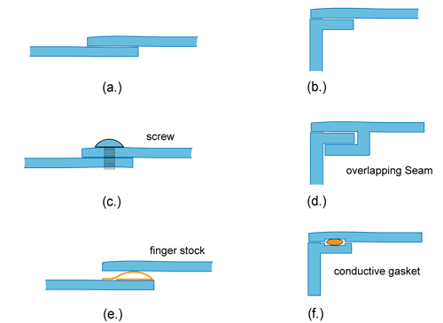
Fig. 7. Seams in shielded enclosures.
Cable Penetrations
In order to power and/or communicate with the electronics in a shielded enclosure, it is often necessary to employ wires that pass through the enclosure wall. A single unshielded, unfiltered wire penetrating a shielded enclosure can eliminate any shielding benefit that the enclosure otherwise provides. As illustrated in Fig. 8, any difference between the voltage on a wire and the voltage on the enclosure drives the wire/enclosure pair like a dipole antenna. Since both wires and the enclosure tend to be among the larger metallic objects in a system, the wire/enclosure pair is often a very efficient antenna at relatively low frequencies.
For this reason, it is very important to ensure that any wires penetrating the enclosure are either:
a.) well-shielded, or
b.) held to the same potential as the enclosure at all frequencies that may be a radiation problem.
 >
>
Fig. 8. Wire driven relative to shielded enclosure.
In order for the shield on a shielded wire to be effective, it must make a low-inductance connection to the shielded enclosure. This is generally accomplished by using a shielded connector that makes a 360-degree metal-to-metal contact with both the cable shield and the enclosure, as illustrated in Fig. 9(a).

Fig. 9. Cable shield to enclosure connections.
A pigtail connection, as shown in Fig. 9(b), will have significant inductance. As a result, any current flowing in the shield will produce a voltage drop across the pigtail that drives the cable shield relative to the enclosure, causing radiated emissions.
If the wires penetrating a shielded enclosure are not shielded, they must be filtered. Filtering will minimize the voltage between the wire and enclosure at radiation frequencies, while allowing low-frequency signals or power to pass unattenuated. It is usually necessary to locate the filter as close to the connector location as possible in order to minimize the inductance of the connections and to prevent the possibility of noise coupling to the filtered wire before it exits the enclosure. Examples of filter locations are illustrated in Fig. 10.

Fig. 10. Possible cable-filter configurations.
Attenuation Due to Waveguides Below Cut-off
Sometimes it is necessary to have a large number of apertures in a shield for the purposes of ventilation. In large enclosures with very stringent shielding and thermal requirements, it may be necessary to further reduce the amount of energy that can escape through any given aperture. This can be accomplished by increasing the depth of the aperture so that it resembles a small waveguide. At frequencies where the cross-sectional dimensions of the aperture are small relative to a half-wavelength, energy propagating through the aperture will be attenuated in the same manner that energy propagating through a waveguide below the cut-off frequency is attenuated.
Energy will not propagate in a waveguide at frequencies below the cut-off frequency. Instead, the fields decay exponentially. A simple approximate formula for the amount of attenuation provided by an opening with depth, d, and maximum height or width, a, is:
(2)
where f is the frequency of the field, and fc is the cut-off frequency of the opening. The cut-off frequency is approximately the frequency at which the maximum height or width, a, is equal to a half-wavelength.
Derivation using a rectangular waveguide
For a rectangular waveguide with height b, width a, and length d, the mode of propagation with the lowest cut-off frequency is the TE10 mode.
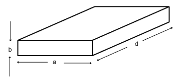
Fig. 11. Rectangular waveguide geometry.
The propagation constant for the TE10 mode is given by,
(3)
At frequencies where the term under the radical is negative, the propagation constant is imaginary, and fields do not propagate. This occurs when λ > 2a. The cut-off wavelength for the TE10 mode is therefore, λc = 2a. The cut-off frequency is,
(4)
where v is the velocity of propagation in the waveguide dielectric (3x10⁸ m/s in air).
Below the cutoff frequency, the magnitude of the field in the waveguide decays exponentially,
(5)
The total attenuation of the field traveling a distance, d, expressed in dB, is then,
(6)
or, combining Equations (3), (4), and (6),
(7)
Derivation using a circular waveguide
For a circular waveguide with diameter a and length d, as illustrated in Fig. 12, the mode of propagation with the lowest cut-off frequency is the TE11 mode.
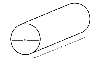
Fig. 12. Circular waveguide geometry.
The propagation constant is given by,
(8)
where kc for the TE11 mode is,
. (9)
Setting the term under the radical in Equation (8) to zero, the cut-off frequency is shown to be,
(10)
where v is the velocity of propagation in the waveguide dielectric (3x10⁸ m/s in air).
Below the cutoff frequency, the magnitude of the field in the waveguide decays exponentially,
. (11)
The total attenuation of the field traveling a distance, d, expressed in dB, is then,
(12)
or, combining Equations (8), (10), and (12),
. (13)
Assumptions and Notes
Note that derivations based on both rectangular and circular waveguides have a constant in front that is within 3 dB of 30. Other modes of propagation yield different constants, but the lower-order modes dominate, so it is reasonable to use a value of 30.
Note that the expression approaches 0 dB as the thickness d of the opening approaches 0. However, even thin apertures will provide some attenuation if their cross sections are small relative to a wavelength. The approximate expression in Equation (2) is not very accurate unless d >> a.
This model does not account for how the field was set up at one end of the opening or how efficiently it is radiated from the other end. Therefore, by itself, it cannot be used to determine the shielding effectiveness of any particular shield. The attenuation calculated in (2) should be added to the shielding effectiveness that would be obtained from the same aperture configuration in a thin shield.
Note that if a wire or second conductor of any kind penetrates the opening, the lowest-order mode of propagation is the TEM mode. Fields at any frequency can penetrate the opening in the TEM mode, so there is no benefit to using a thick aperture if a wire penetrates the aperture.
Some textbooks state that the attenuation in (2) should be reduced by a factor of 10*log10(# of apertures) if there are multiple apertures. However, the attenuation in Equation (2) is in addition to any attenuation provided by a thin aperture or an array of thin apertures. Equation (2) cannot be used to calculate the shielding effectiveness directly, and there is no reason to reduce the Equation (2) value for multiple thick apertures if you are starting from the attenuation provided by multiple thin apertures.
References
[1] H. Ott, Electromagnetic Compatibility Engineering, John Wiley & Sons, New York, 2009.
[2] C. R. Paul, Introduction to Electromagnetic Compatibility, 2nd Ed., Wiley Series in Microwave and Optical Engineering, 2006.