PCB Layout
Some circuit designs are fabricated on tiny silicon wafers, and others consist of various components connected by cables. However, the circuits that are often the center of an EMC engineer’s attention are those that are laid out on cardboard or fiberglass epoxy boards. Printed circuit boards like the one illustrated in Figure 1 can be found in nearly all electronic systems. Circuit components with metal pins are connected by copper traces. Surface-mount technology (SMT) components are glued to the top and/or bottom of a board. Pin-in-hole components are held to the board by their pins, which extend through the board and are soldered to traces on the opposite side.
Single-layer boards have all the traces routed on one side of the board. Double-layer boards have traces on both sides. Many boards have several layers of copper traces separated by layers of fiberglass epoxy (or a similar dielectric). These are referred to as multi-layer boards. The number of layers is usually even. Four-layer boards are very common in low-cost products. Boards with dozens of layers are sometimes used to connect densely populated boards with high component pin counts.
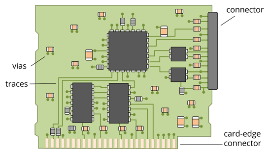
Figure 1: A printed circuit board.
Multi-layer boards often have entire layers with solid copper planes dedicated to the distribution of power to the components on the board. These planes provide a low-impedance path for the DC power currents, as well as a return-current path for single-ended signals.
The placement of components and the routing of traces usually play a crucial role in determining the electromagnetic compatibility of products employing printed circuit boards. Well-laid-out boards will not radiate significantly on their own, and they do a good job of minimizing currents and fields that might couple noise to cables or other objects off the board. They are also configured to minimize opportunities for external currents or fields to couple interfering signals onto the board.
Strategies for Laying Out Printed Circuit Boards
Many board designers employ a list of guidelines to help them place components and route traces. For example, a typical guideline might be “minimize the length of all traces carrying high-speed digital signals.” That might be good advice in general, but long traces carrying high-speed digital signals do not necessarily cause a problem. High-speed digital signals are routinely routed across large boards, or even between boards, without any EMC or signal integrity problems. So, exactly how important is it to minimize the length of these traces? Often, a designer is not familiar with the reason for the guideline or does not fully understand the consequences of violating the guideline for a particular application. And often, boards laid out by people trying to adhere to a long list of EMC guidelines are worse than boards laid out by people with no EMC guidance at all.
For example, suppose someone is laying out a high-speed multi-layer printed circuit board and needs to route a trace carrying a high-frequency signal from a digital component to an analog amplifier. They want to minimize the chance of having an EMC problem, so they search the web for EMC design guidelines and find three guidelines that seem to pertain to their situation:
- minimize the length of high-speed traces,
- gap any solid planes between analog and digital circuits, and
- never let a high-speed trace cross over a gap in the signal return plane.
They envision three possible routing strategies as illustrated in Figure 2. The first option routes the trace directly between the two components but leaves the plane between them solid. The second option gaps the plane but routes the trace over the gap. The third option routes the trace around the gap. Each of these alternatives violates one of the guidelines.
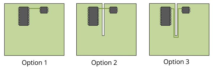
Figure 2: Which is the best trace routing alternative?
Is each alternative equally good because it satisfies 2 of 3 guidelines? Are they all bad because they all violate at least one guideline? Making the right choice can be the difference between a board that meets all requirements and a board that has severe radiated emissions or immunity problems. In this example, Option 1 would almost always be the correct choice. The guideline to gap ground planes between analog and digital components is usually terrible advice, but it is still found in some texts and many internet sources.
There are no EMC design rules that can be applied in every situation. Blindly adhering to a list of EMC design rules is not likely to result in an EMC-compliant design. The best strategy for designing and laying out EMC-compliant printed circuit boards involves identifying and quantifying possible sources, victims, and coupling paths.
In this tutorial, we will explore the steps that every EMC engineer should follow when laying out a printed circuit board or reviewing an existing board design. These steps include:
- Identify potential EMI sources and victims,
- Identify potential antenna parts,
- Explore possible coupling mechanisms.
By recognizing the design decisions that could make a difference in an EMC compliance test, the impact of component placement and trace routing decisions becomes clear. It becomes immediately apparent which design guidelines are important and which are not important at all for a specific board design.
Identifying Potential EMI Sources and Victims
A typical circuit board may have dozens, hundreds, or even thousands of circuits. Each circuit is a potential source of energy that might eventually be coupled unintentionally to other circuits or devices. Each circuit is also a potential victim of unintentionally coupled noise. However, some circuits are much more likely than others to be a noise source, and other circuits are much more likely to be victims. EMC engineers (and board designers) should be able to recognize those circuits that are potentially good sources and those that are potentially most susceptible. Circuits of particular interest are discussed below.
Digital Clock and Signal Circuits
Synchronous digital circuits employ a system clock. Clock signals are constantly switching and have narrow-band harmonics. They are often among the most energetic signals on a printed circuit board. For this reason, it is not uncommon to see narrow-band radiated emission peaks at harmonics of the clock frequency, as illustrated in Figure 3.
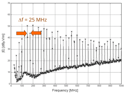
Figure 3: Radiated emissions from a product with a 25-MHz clock.
In this figure, the radiated emissions are dominated by harmonics of a 25-MHz clock. The noise floor from 200-1000 MHz is the thermal noise of the spectrum analyzer used to make the measurement (corrected to reflect the antenna factor). To make this product compliant with the FCC or CISPR Class B radiated emission specification, the amplitude of the source harmonics could be decreased, the unintentional “antenna” could be made less efficient, or the source-antenna coupling path could be attenuated.
Digital signals are not necessarily as periodic as clock signals, and their random nature results in noise that may be more broadband. Digital signals that toggle more often can result in radiation emission profiles similar to clock signals. An example of this would be the least significant bit on a microprocessor address bus, since stepping through consecutive addresses can cause this signal to toggle at the clock frequency. The exact form and strength of the radiation from digital signals depend on many factors, including the software running and the encoding scheme employed. Generally, data signals are a less troublesome source than clock signals; however, high-speed data can still produce significant amounts of noise.
Analog Signals
Analog signals can be broadband or narrowband, high frequency or low frequency. If your board employs analog signals, it is a good idea to be familiar with how these signals look in both the time and frequency domains. Narrowband, high-frequency analog signals can be strong emission sources. Fortunately, it’s relatively easy to control the path of these signal currents because they will take the path of least inductance and minimize their own loop areas. Low-frequency analog signals can be more problematic because the signal current paths are less well contained. These signals may be vulnerable to interference from other low-frequency sources sharing the same current path. For both high- and low-frequency analog signals, it’s important to follow the current and evaluate the coupling to and from the signal path.
Power Switching Circuits
Switch-mode power supplies, DC-DC converters, and power inverters generate different voltages by rapidly switching the current into an inductor or transformer on and off. Typical switching frequencies are in the 10-100 kHz range for high power inverters and 1-10 MHz for lower power DC-DC converters. The spikes of current generated by this switching can put noise on the power distribution nets and couple to other devices and circuits on the board. Although this noise is relatively periodic, producing narrow-band harmonics, it can appear as broadband noise in a conducted or radiated emissions test if the switching frequency is lower than the resolution bandwidth of the measurement.
The small hump in the noise floor around 120 MHz in Figure 3 is due to power switching noise. In this product, the switching noise is negligible relative to the clock noise. However, in other products, the power switching noise can dominate.
Power switching noise can be reduced by slowing down the transition time of the switching circuit. However, transition times that are greater than about 1% of the switching period can noticeably reduce the efficiency of the power supply. Field-coupled noise from switching power circuits is typically mitigated by keeping the switch nodes and switching current loops away from nearby circuits that might carry the noise away from the immediate area. Conducted coupling is generally controlled by carefully selected and located filter components.
DC Power Traces and Low-speed Digital Signals
DC power and low-speed digital signals do not usually have enough power at radiated emission frequencies to be troublesome. Nevertheless, DC power and low-speed digital signal conductors often carry strong high-frequency currents that can be a significant source of radiated emissions problems. The source of these currents is typically the high-speed components connected to these conductors. In some cases, the clock-frequency currents on nominally low-frequency traces can exceed the clock-frequency currents on the clock traces.
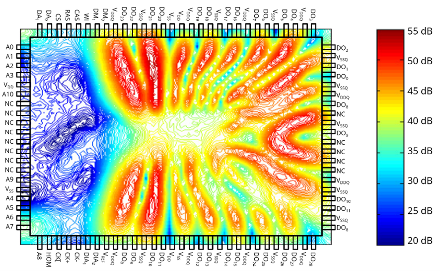
Figure 4: Near magnetic field above a packaged integrated circuit.
Figure 4 shows a map of the near magnetic field above a dynamic random access memory module. The near magnetic field provides an indication of the currents flowing in the lead frame of the component package. The frequency of the measurement is the third harmonic of the clock frequency. Note that more current is being drawn from the DC power supply pins than is being drawn from the signal pins.
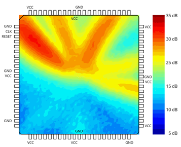
Figure 5: Near magnetic field above a microprocessor.
Figure 5 shows a similar plot of the near magnetic fields above a microcontroller implemented in a field programmable gate array (FPGA). The field was measured at the fundamental clock frequency. In this case, the strongest current is on the clock trace. However, currents of similar amplitude are flowing in some of the connections to address lines across the top.
Why do high-frequency currents and voltages appear on low-frequency data lines? There are several ways that this can happen, depending on the design and layout of the integrated circuit (IC). Some ICs do a good job of containing their internally generated noise, and others do not. A poor design can put high-frequency voltage fluctuations on every input and output trace connected to the IC. And even good designs tend to put significant amounts of current on some of the I/O pins at harmonics of the internal clock frequencies.
When laying out a printed circuit board with an IC that is clocked internally at a high frequency, it is a good idea to treat every pin on that IC as if it were a high-frequency source with the same characteristics as the internal clock. Otherwise, some of the power or low-speed digital traces connected to the IC could provide a conduit for high-frequency noise coming from the IC.
Wide-bandwidth, High-gain Amplifiers
It is also important to identify potential victim circuits to anticipate potential EM immunity problems with the board layout. Almost all of the circuits in a typical board are potentially vulnerable to large transients or strong RF noise, but wide-bandwidth, high-gain amplifier circuits deserve particular attention. This includes circuits that contain op-amps, even if the surrounding circuitry limits the nominal bandwidth and/or gain. Amplifiers with a wide bandwidth are generally sensitive to noise in a wide range of frequencies, including frequencies outside the nominal signal bandwidth. High-gain amplifiers can be sensitive to small amounts of coupled noise, and a moderate amount of noise can saturate the amplifier, resulting in the generation of strong signal harmonics.
Identifying Antennas/Ports
To fail a conducted or radiated emissions test, signals or noise generated on the board must be coupled off the board. To fail a conducted or radiated immunity test, signals or noise originating off the board must be coupled onto the board. Identifying the unintentional antennas or “ports” that facilitate the coupling of noise to and from the circuit board is a key part of any EMC design review. To meet radiated emissions and immunity requirements, it is important to identify the structures that will ultimately be the unintentional antennas. This includes structures that may not be located on the board, but instead are driven by the board (e.g., cables and connections to the enclosure). To meet conducted emissions requirements and immunity requirements, including ESD, EFT, and BCI, it is important to identify the ports (e.g., connectors or access points) that will bring interference onto or off from the circuit board.
Unintentional Antennas
As described in the section on electromagnetic radiation, there are basically 3 conditions that must be met for most of the unintentional antennas that an EMC engineer encounters to radiate effectively.
- The antenna must have two parts.
- both parts must not be electrically small.
- something must induce a voltage between the 2 parts.
Most printed circuit boards are electrically small at frequencies below about 100 MHz (λ > 3 meters). This implies that any efficient antenna parts must be relatively large compared to most of the board components. Generally, at low frequencies, the only viable antenna parts are the attached cables and/or a metallic chassis. If a printed circuit board is laid out in a manner that minimizes the possibility of inducing a voltage between any two of these possible antenna parts, then it is much less likely to have a radiated emission or radiated susceptibility problem.
Figure 6 shows two printed circuit board layouts. In both layouts, the connector and chassis connections represent possible efficient antenna parts. It’s important to hold all the antenna parts to the same potential. As little as 1 mV driving one antenna part relative to another could cause a radiated emissions failure. In Layout #1, Connector 1 is located on the opposite side of the board from Connector 2 and the chassis connections. It would be difficult to keep the circuits on the board from driving one connector relative to the other.
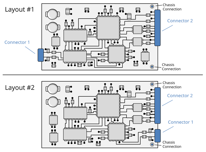
Figure 6. Two printed circuit board layouts.
Layout #2 is much less likely to have radiated emissions or immunity problems, because it would be much more difficult to develop a significant voltage between any two conductors capable of serving as an efficient antenna. In fact, locating all the I/O connectors on one side of a board is often an important first step in guaranteeing emissions and immunity compliance. This is especially true if the board does not have a metal chassis or enclosure to establish a high-frequency reference for all external connections.
At frequencies above 100 MHz, wavelengths are shorter, and it becomes more likely that objects mounted on the board (or the board itself) can serve as efficient antenna parts. Nevertheless, even at frequencies up to several GHz, these antenna parts should be relatively easy to spot. For example, at 1 GHz, the wavelength in free space is 30 cm. A quarter wavelength is 7.5 cm. Therefore, an efficient antenna part will have to be at least several centimeters long and be driven relative to something that is just as large or larger.
Recall that differential currents (currents with nearby return paths) are relatively inefficient radiation sources. This means that a trace that is right beside or above its current return path is not a good antenna part. So, if one half of our antenna is a metallic plane in the board, the other half must stick up and away from the plane. This helps to make these antenna parts readily identifiable even at high frequencies. Table 1 lists common antenna parts found on printed circuit boards above and below 100 MHz.
|
Good Antenna Parts
|
Poor Antenna Parts
|
||
|
< 100 MHz
|
> 100 MHz
|
< 100 MHz
|
> 100 MHz
|
|
cables or cable shields
|
tall components or heatsinks
|
integrated circuits
|
integrated circuits
|
|
metal enclosure or chassis
|
seams in shielding enclosures
|
microstrip or stripline traces
|
microstrip or stripline traces
|
|
|
sparsely populated power planes
|
anything that is not big
|
densely populated power planes
|
Identifying and Quantifying the EM Coupling
Once we have identified the potential sources or victims and the potential antennas/ports, a good board layout is simply a matter of controlling the coupling between the two. Earlier, we learned that there are 4 possible electromagnetic coupling mechanisms:
- Conducted coupling,
- Electric field coupling,
- Magnetic field coupling, and
- Radiation.
On a circuit board, the coupling between a source and its antenna/port will not be radiation coupling, so there are only three coupling mechanisms that we need to consider.
Conducted Coupling
Conducted coupling will only occur if the source is directly connected to and drives one good antenna part relative to another. Two examples of conducted coupling are illustrated in Figure 7. Figure 7(a) shows a single-ended signal being transmitted on an unshielded twisted wire pair. A common-mode voltage is developed between the unbalanced driver and the balanced cable. This voltage drives the cable relative to the board and chassis connections.
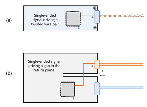
Figure 7: Two examples of conducted coupling driving an antenna structure.
Figure 7(b) illustrates a single-ended signal trace crossing over a gap in the return plane. The impedance in the path of the return current generates a voltage across the gap. This voltage drives cables referenced to one side of the gap relative to cables referenced to the other side.
Conducted coupling tends to be easy to spot once the source and the antenna parts have been identified. By simply paying attention to the high-frequency current paths, conducted coupling between intentional signals and unintentional antennas can usually be avoided.
Electric Field Coupling
An example of how electric field coupling can produce radiated emissions is illustrated in Figure 8. A large heatsink is mounted over an integrated circuit. As the IC pulls current from the power and ground at high frequencies, it takes on a voltage relative to the plane below it. At frequencies where the heatsink is not electrically small, it is potentially an effective antenna part. Electric-field coupling from the surface of the IC drives the heatsink relative to the board planes. As little as 1 mV between the heatsink and board at the structure’s resonant frequency can cause a radiated emissions failure.
Another way that the structure in Figure 8 can cause radiated emissions is for the field from the heatsink to couple to nearby circuit board traces. These traces can carry noise to other areas of the board. If the traces connect to wires that leave the board, those wires can be driven relative to the board and chassis grounds.
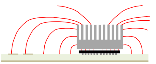
Figure 8: Integrated circuit package coupling to a heatsink.
When heatsinks are very large, it’s sometimes necessary to route traces directly beneath the heatsink. In this case, the electric field coupling to the trace can be very strong, as much as half the noise voltage on the IC itself. If this noise cannot be tolerated, traces should be routed on a layer beneath the uppermost circuit board plane.
Note that grounding the heatsink to the uppermost plane would reduce its voltage relative to the plane. This would reduce any electric field coupling from the heatsink. Unfortunately, it is often challenging to establish a low-impedance bond between a heatsink and a circuit board plane at high (e.g., GHz) frequencies. In many cases, it is better to minimize the size of the heatsink and keep unnecessary traces and components a safe distance away.
Of course, electric field coupling doesn’t have to involve heatsinks. Any component or trace with a high-frequency voltage relative to the board ground can be the source of electric field coupling. The switch nodes of DC-to-DC converters and motor drivers are common examples of circuit board traces that can strongly couple to nearby traces or components and carry that noise to unintentional antennas. A worst-case analysis of this coupling can determine whether it is likely to couple enough noise to be a problem. If so, the coupling can be reduced by layout changes or (in some cases) using board-level electric field shielding.
Magnetic Field Coupling
Figure 9 illustrates a very common magnetic field coupling problem in many printed circuit board designs. An otherwise well-designed board has connectors attached to each side. A circuit consisting of a single microstrip trace driven at one end and terminated at the other end is located between the two connectors.
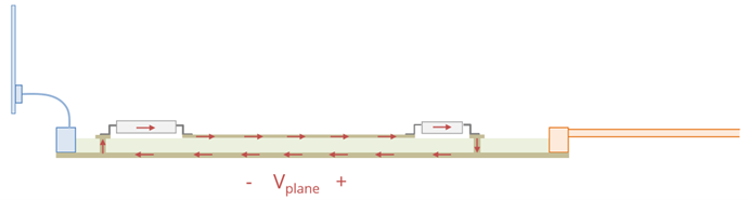
Figure 9: Example of magnetic field coupling on a circuit board.
Microstrip traces are not efficient radiated emission sources, so the only possible antenna parts in this design are the two connectors and their attached cables. One might expect the two antenna parts to be at the same potential, because they are connected to each other with a wide copper plane. However, an important requirement for a “ground” conductor is that it does not carry intentional power or signal currents.
The “ground” plane in this design does carry signal currents. In fact, the current flowing in the plane generates a magnetic flux that wraps around the plane. The flux wrapping the plane effectively produces a voltage that can drive things referenced to the plane on opposite sides. This voltage is difficult to quantify precisely because it depends on many factors, including the position and orientation of the cables. Nevertheless, a general rule of thumb is that tens of milliamps at tens of megahertz will effectively induce millivolts of voltage. Increasing the trace width or trace height increases this voltage, while stripline traces with currents returning above and below the trace produce no voltage at all.
A good way to avoid this problem is to make all the external connections on one edge of the board. Then, provided no high-speed traces are routed near and parallel to the edge, the plane will provide a good reference ground.
Another option when high-speed circuitry must be located between connectors is to mount the board on a metal chassis that makes a good connection to the board's ground plane on both sides. This effectively shorts out the voltage induced across the plane, and currents can circulate harmlessly on the chassis.
Crosstalk to an I/O Trace
Although strictly speaking, it is not an independent coupling mechanism, another common problem that occurs with printed circuit board layouts is inadvertent crosstalk between signal traces and I/O traces capable of carrying that noise off the board. An example of this is illustrated in Figure 10. A moderately high-speed trace is routed alongside another trace that attaches to a connector. Voltages and/or currents coupled from one trace to the other (via electric or magnetic fields) can be propagated down the I/O trace and off the board. This coupling effectively drives the cable relative to the board and chassis ground.
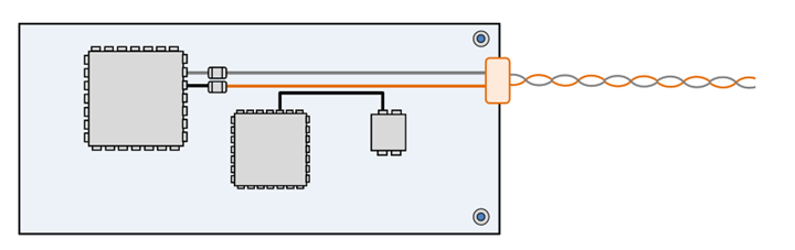
Figure 10: Example of crosstalk to an I/O trace.
This problem is usually obvious once you see it. However, on a board with hundreds or thousands of traces, this situation arises more often than it should. If the board layout software can’t check for I/O traces that are routed in the vicinity of high-speed traces, then this should be done manually. The same also applies to I/O traces routed in the vicinity of traces connected to vulnerable inputs, since the easiest way for radiated noise to get onto a board is through the I/O.
Printed Circuit Board Design Review
Now that we know a little more about noise sources, antennas and coupling mechanisms on printed circuit boards, let’s look at some of the steps that can be taken to systematically review a printed circuit board design. We’ll assume we have circuit schematics and a preliminary board layout available. We may also need component datasheets and physical descriptions of the various signals on the board and the I/O. Finally, we’ll need to understand the product’s function, grounding strategy and EMC requirements.
The design review steps provided here are intended to provide general guidance concerning things to look for and basic methods for determining when something must be changed. They are presented in a specific order that generally works well, but may not be optimum in all situations. It’s more of a checklist rather than a set of step-by-step instructions.
1. Identify connections to the ground structure and the locations of all I/O.
An essential part of making good EMC design decisions is understanding where your board’s EMC ground is located. Basically, all the I/O will be bonded to (or referenced to) this ground at high frequencies. Any I/O that can’t be bonded to ground must be filtered, shielded, or isolated, or we must be able to demonstrate that the ungrounded I/O cannot possibly contribute to an EMC compliance problem.
If the board carries high-speed signals and does not have a metal chassis, it’s important to put all the connectors on one edge or in one corner if possible. If high-speed circuitry must be located between connectors, then there must be a plan in place to prevent one cable from being driven relative to another.
2. Identify ground plane layer(s) and the extent of the plane.
Ideally, the board has enough solid ground (current-return) planes to ensure that high-frequency return currents come back directly above and/or below the signal trace. These planes should not be gapped for any reason, although the plane may not need to extend to areas of the board where it is not utilized.
3. Identify ground traces or fills on other layers.
A board with solid ground planes should usually not have ground traces or ground fill on other layers. When a connection needs to be made to ground, it should be made with a via connecting directly to the plane. Any component that connects to a ground trace or ground fill does not necessarily have a low-inductance connection to the ground plane. And sometimes the presence of a ground trace or fill indicates that two or more components are sharing a connection to ground. Sometimes we can get away with this, but it’s not optimal. Ground traces and ground fills serve a useful purpose on boards with 1 or 2 layers, but they should not be present on most multi-layer boards with solid ground planes.
4. Identify power distribution layer(s) and the type of power distribution.
If the board has active components with three or more power pins at a given voltage, that voltage should probably be distributed on a closely spaced (i.e., < 0.25 mm) pair of planes. High-frequency decoupling capacitors should be mounted on the side of the board closest to the plane pair. If the active components have only one or two power pins, power can be routed on planes or traces. The decoupling should be appropriate for power distribution geometry as described in the Power Bus Decoupling section of these course notes.
5. Identify the I/O nets.
With board layout viewers, it’s easy to highlight each net attached to a connector pin. These are the nets that will carry emissions noise off the board and/or bring interfering signals or transients onto the board. Ideally, these nets terminate in a series component near the connector. Follow each I/O net and look for possible ways that noise might couple to or from the trace. If there is a potential coupling problem, do a worst-case coupling calculation to determine if a layout change is required.
If the I/O net connects directly to an IC, make sure signals or noise from the IC can’t drive the I/O with more than about 1 mV of common-mode voltage. If necessary, provide filtering and/or transient protection on the net.
6. Identify filter components.
Filters play an important role in EMC compliance. Look for filter components to ensure they are well-mounted to minimize parasitics and prevent inadvertent coupling that would bypass the filter. Make sure that higher-order filters are designed appropriately and won’t ring at their cut-off frequency. If the filter has an inductor, determine whether it needs to be shielded. If the filter uses ferrites, check the datasheet to be sure they are appropriate for that application. If the filter employs a common-mode choke, make sure it is filtering a balanced pair of signal or power conductors.
7. Identify traces requiring transition-time control with series resistance.
By default, it is a good idea to assume every digital signal trace driving a capacitive load needs a series resistor to control its transition time. Then, remove the resistor from any trace where it is clearly not required. The most common reason for removing the transition time control resistor is when you can follow the trace current from end to end and see clearly that there is no opportunity for coupling to another trace that would carry signal noise to a victim circuit or to an unintentional antenna. If there is any doubt, do a worst-case coupling calculation.
The transition time of signals on controlled impedance traces with matched terminations should be controlled using logic with a controlled slew rate. If that logic is not available, the signal should be filtered, or the traces should be well-isolated from anything that could couple noise in or out of the signal path.
8. Identify critical components.
Some components on a circuit board require special attention during the design review. For example, inductors are generally associated with filters, power converters, or RF circuits. Each of these applications requires a little extra attention during layout. Identifying the inductor locations helps to focus attention on regions where the board layout can be critical.
Analog amplifiers (particularly op-amps) are another type of component with special layout concerns. Op-amps inherently have high gain and a wide bandwidth. Small amounts of noise coupled to the input or feedback loop of an op-amp can disrupt the entire circuit. Ensure that the loop areas associated with the input and feedback components are small. Make sure the traces are routed over a solid ground plane and do a worst-case calculation of the coupled E-fields and H-fields that would occur during an immunity test.
Transient protection components are also critical. Make sure they are chosen appropriately for the application. Also, be sure they connect to the correct “ground.” Components protecting IC inputs should be connected to the IC ground. Components protecting the board should be connected to the EMC ground. For fast transients, the inductance of the connection is critical. Be sure the time it takes for the transient protection to turn on is faster than the time it takes for a component to be damaged.
Phase-locked loops (e.g., as used in clock multipliers) are very sensitive to small amounts of power bus noise. Some ICs that employ multipliers have certain power inputs that require filtered power. Often, this is accomplished with a ferrite on the power input. It’s generally a good idea to follow the recommendations of the IC manufacturer, but never put a ferrite on the ground connection.
When ferrites appear in series with traces that are not carrying DC power, check to ensure that a ferrite is the right choice. For capacitive loads, resistors are usually a much better option. If the ferrite is on a ground or a single-ended signal-return conductor, it should probably be removed.
9. Identify power inverter circuits/devices.
Locate the switching voltage nodes and minimize their surface area. Keep them away from any conductors that might carry the switching noise away from the immediate area. Identify the switching current loops and look for magnetic field coupling to nearby circuits that could carry the switching noise away.
Watch for unintended coupling from the components as well as the traces. Do a worst-case calculation of this coupling and use shielded components if necessary.
Power converters that have come out in the past few years tend to be much smaller and quieter than older converters. Low to medium-power DC-to-DC converters should be switching at frequencies in the MHz range. They should not have isolated power grounds. Many of the converters available today have EMI-reducing features such as controlled slew-rates, spread-spectrum switching, and optimized pin layouts. Take advantage of these features and don’t stick with older components just because they have been good enough in the past.
Finally, if the power converter is in the vicinity of an intentional receiving antenna (e.g., GPS or Wi-Fi), board-level shielding may be required to reduce coupling from the converter that could impact the signal-to-noise ratio of the receiver.
10. Identify currents and coupling for each EMC compliance test.
As a final check of the board layout, it’s a good idea to review each EMC compliance test requirement and visualize the impact of the layout on that test. For example, if the board will be tested for conducted emissions, identify the most likely noise sources and follow the EM coupling paths that could bring that noise to the LISN. Do a quick, worst-case calculation for any coupling that looks like it could cause a compliance problem. Ensure that the power input filter will have sufficient insertion loss at the required frequencies.
Similarly, for radiated emissions, identify the most likely noise sources and evaluate the worst-case coupling to potential antenna structures. Don’t try to calculate radiated field strengths, but ensure that no two antenna parts can be driven by a millivolt or more at any radiated emissions test frequency. For emissions requirements more stringent than CISPR 32 Class B, this voltage might need to be as low as 100 microvolts.
If the board will be subjected to a bulk current injection test, follow the current as it comes in on the harness and makes its way to the metal tabletop. Be sure there is a low impedance path and watch for any EM coupling that might occur to vulnerable components or circuits. Evaluate the worst-case coupling to ensure that the board will not have any trouble complying with this test.
For radiated immunity tests, follow the same procedure used for the bulk current injection test. In addition, if the board is not in a metal enclosure, evaluate the worst-case coupling that could occur directly from the fields to vulnerable circuits.
If the board will be subjected to electrical fast transients, model the source to determine the worst-case current waveform. Follow the current from the harness to the place where it will leave the board. Watch for coupling that might result in a failure to comply with the test requirement. Add transient protection or filtering if necessary.
If the board is in a metal enclosure, the ESD currents are most likely to come in on connector pins. Follow the current on any I/O nets that will be subjected to an ESD test. Use blocking resistors or transient protection circuits to protect any components that may not survive a direct discharge. Make sure the ESD current flows to the metal enclosure without being pulled too far onto the board.
If the board is in a plastic enclosure, look for possible arc paths through seams or openings in the enclosure. If the path cannot be blocked, be sure the ESD current can get to the board’s EMC ground without being pulled onto the board. Also, boards in a plastic enclosure will experience strong field coupling during the initial part of the transient. Make sure that short, low-energy voltage spikes coupled to any of the circuits will not cause an unacceptable ESD failure. Use resistors to slow the response time of high-impedance digital inputs. Verify that any high-speed data errors will be detected and corrected.
By visualizing each EMC test and the path of the relevant currents, potential compliance issues often become obvious. This allows board designers to address them before the first prototypes are built and tested. And even in situations where compliance vs. non-compliance is not clear, the visualization exercise allows the designer to anticipate possible problems. In these situations, mounting pads and clearances can be incorporated in the design to allow for filtering, transient protection, or shielding in the event that it is necessary.