Identifying Current Paths
Electrical engineers are generally more comfortable thinking of electrical signals in terms of voltage rather than current. Digital logic levels are normally determined by signal voltages, and power supplies are generally constant voltage sources. Voltages in a circuit can usually be measured using simple probes without loading the circuit significantly.
Currents, on the other hand, are more difficult to measure. Typically, current is measured by passing it through a small resistance and measuring the voltage dropped across the resistance. Alternatively, we measure the voltage induced in a loop by the magnetic field accompanying the current. In many circuit designs, maximum currents are specified, but little attention is paid to current waveforms or current paths.
Quiz Question
The ultimate destination of the signal current that flows out of a pin in an integrated circuit is,
- earth ground
- the ground plane of the printed circuit board
- one or more of the other pins on the integrated circuit
One of the most important skills that an EMC engineer must develop is the ability to identify both the intentional and unintentional currents in an electronic system. Current is primarily responsible for 3 of the 4 possible EMC coupling mechanisms described in the first chapter. Without understanding how and where the currents in each circuit flow, it can be difficult to anticipate problems in new designs or fix problems in existing designs.
The first rule to remember when identifying the path of a current is that all currents return to their source. In other words, currents flow in loops. Yes, there are displacement currents (i.e., time-varying fields that result when the net charge on a conductor changes). However, net charge cannot be created or destroyed, and the current (i.e., the sum of conduction and displacement current) flowing out one side of a device must equal the current flowing in the other.
Digital circuit designers often neglect to consider where the currents in their designs will flow. It is not uncommon to see the current path from the signal source to the load very carefully laid out, while the path from the load back to the source is left to chance.
Many years ago, EMC engineers at IBM were evaluating a product that had severe electromagnetic susceptibility problems. The system employed an 8-bit communication bus that was routed on a cable between two boxes. When the EMC engineers examined the cable, they found that it had exactly 8 wires (one for each signal, but none for returning the signal current). The product designer explained that the signals were voltages referenced to the chassis ground of each box. What the product engineer didn't realize was that the signal return currents had to flow through the chassis, then the power cable, then through the building wiring, then through the power cable and chassis of the source box. This relatively high-impedance path caused the chassis of the two boxes to be at different potentials. In addition, the large loop area associated with the signal current path was capable of receiving significant amounts of electromagnetic noise.
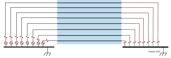
Figure 1: An 8-bit data bus with no explicit signal return path
However, this was not the whole story. As illustrated in Figure 1, the chassis/building ground was one possible signal current return path, but it was not the only one. In this case, the current in any signal wire also had the option of returning to the source through the other signal wires. For example, suppose in this case that a logic "1" was represented by a positive 5 volts on the signal line and a logic "0" was represented by 0 volts. Then, at any given time, the current from the logic "1" lines could return to the source through the logic "0" lines. In order for this to happen, the current from logic "1" lines would flow through their own load resistances and then through the load resistances of the logic "0" lines, inducing a negative voltage across these loads.
Whether the currents would return to their respective sources through the chassis ground or through the other signal lines would depend on the relative impedance of these two options. The second rule to apply when identifying the path of a current is that current favors the path(s) of least impedance.
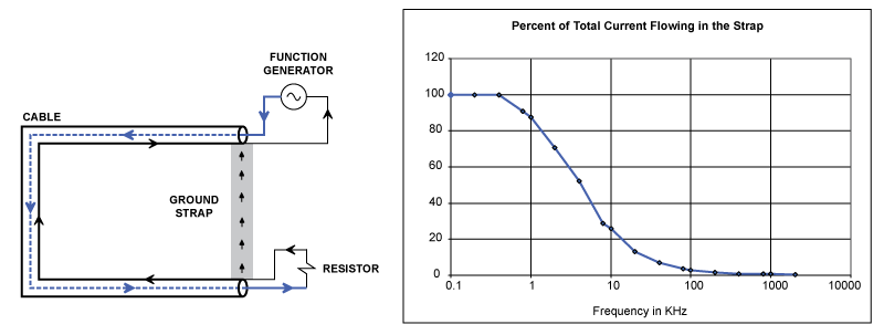
Figure 2: A simple current path demonstration.
Consider the configuration illustrated in Figure 2. A variable frequency source places a voltage across the input to a coaxial cable. Signal current flows through the cable along the inner conductor of the coaxial cable, then through the resistor. At that point, there are two possible paths that the current can take to return to the source. Current can take the shortest path through the copper bar, or it can flow along the shield of the coaxial cable.
At low frequencies, the impedance of the current path is primarily determined by the resistance of the conductor. Since the shorting bar has a lower resistance than the coaxial cable shield, most of the current flows in the bar. However, when current returns through the bar, the loop area of the current path is relatively large. The impedance of the current path is approximately R + jωL, where R is the conductor resistance, and L is the path inductance.
At high frequencies, the inductance becomes a more important parameter than the resistance, and the path of least impedance is the path of least inductance. Therefore, at high frequencies, current returns on the cable shield. This path minimizes the loop area and is therefore the path of least inductance.
In the example in Figure 2, the frequency at which the resistance and the inductive reactance are equal is about 5 kHz. The exact cut-off frequency will depend on the materials and the geometry of the path. However, for most practical circuit configurations, the path of least impedance will be the path of least resistance at kilohertz frequencies and lower. It will be the path of least inductance at megahertz frequencies and higher.
Consider the printed circuit board illustrated in Figure 3. Signal current from an output pin of Device 1 flows through a copper trace to an input pin of Device 2. We'll assume the current into Device 2 comes out the pin labeled "GND" and the current into Device 1 comes in the pin labeled "GND" and that both "GND" pins are connected to a solid copper plane on the board. What is the current return path in this situation?
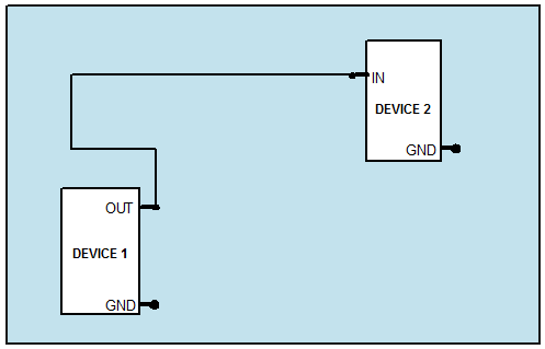
Figure 3: A simple printed circuit board with two components.
Figure 4a illustrates the current distribution on a conducting plane under a microstrip trace when the current takes the path of least inductance. Note that most of the current returns in a band that is only a few trace heights wide. At megahertz frequencies and higher, the inductance will determine the current return path, and currents will flow on the ground plane primarily in a narrow path directly under the trace, as indicated in Figure 5a.
Figure 4b illustrates the current distribution on a plane when the resistance of the plane is the dominant contributor to the path impedance. The current density is essentially uniformly distributed across the plane and inversely proportional to the width of the plane. Viewed from the top, as illustrated in Figure 5b, the current spreads out from the point where it is deposited on the plane and comes together again at the point where it leaves the plane.
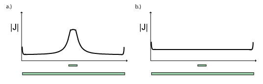
Figure 4: Current density on the surface of a plane beneath a microstrip trace, a.) when the inductance dominates, and b.) when the resistance dominates.
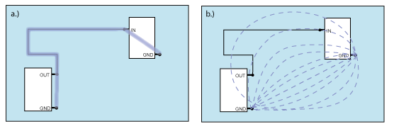
Figure 5: Current path on the plane of the board in Figure 3, a.) at MHz frequencies and above, and b.) at kHz frequencies and below.
Example 1: Identifying Current Return Paths
For each of the configurations illustrated in Figure 6, identify the primary return current paths.
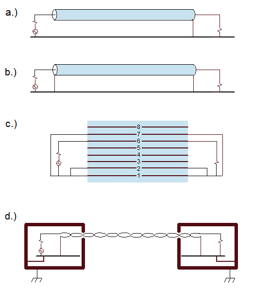
Figure 6: Signal transmission configurations for Example 1.
In the first configuration above, there is only one possible path for the return current to take. Therefore, all low-frequency and high-frequency currents must return on the metal surface. In the second configuration, the cable shield grounded at both ends provides an alternative return path. Currents at megahertz frequencies and higher will return to the source on the shield of the coaxial cable. Kilohertz and lower frequency currents will distribute themselves between the two conductors based on their relative resistances.
For the ribbon cable configuration, low-frequency currents will return primarily on wires 1, 2 and 7 with an equal amount of current on each wire. High-frequency currents will return primarily on wire 7.
The last configuration illustrates two devices communicating with a twisted-wire pair. The signal current flows out one wire in the pair and, at high frequencies, returns on the other wire in the pair. However, at low frequencies, a significant fraction (perhaps most) of the current will return through the chassis grounds of each device. This unintended return path can result in a variety of EMC problems.