Grounding
Proper grounding is an important aspect of electronic system design for both safety and electromagnetic compatibility. Ground plays a crucial role in determining what happens in the event of unintentional faults, electrical transients, or electromagnetic interference. Proper grounding strategies also enable engineers to control unwanted radiated emissions more effectively.
Improper grounding, on the other hand, can undermine the safety and the electromagnetic compatibility of a product or system. In the past few decades, poor grounding has become a leading contributor to EMC-related system failures.
Developing a good grounding strategy is a straightforward process. So, one might wonder why so many systems are improperly grounded. The answer is simple: engineers often confuse the concept of ground with another important concept, current return. The fact that current return conductors in digital electronics are often labeled ground or GND can be confusing. When current return conductors are treated like grounding conductors (or when grounding conductors are used to return currents), the result is often a design with significant EMC problems.
Definition of Ground
4.152 – grounding. (1) The bonding of an equipment case, frame, or chassis to an object or a vehicle structure to ensure a common potential. (2) The connecting of an electric circuit or equipment to earth or to some conducting body of relatively large extent that serves in place of earth.
It was well understood that ground was a reference potential and that ground conductors were normally non-current-carrying conductors.
In the U.S., 110-volt grounded outlets have three terminals, as shown in Figure 8.1. The hot terminal has a nominal potential of 110 Vrms and supplies power current. The neutral terminal has a nominal potential of 0 Vrms and acts as the power current return. The ground terminal also has a nominal potential of 0 Vrms but does not carry current under normal conditions. The neutral and the ground terminals are both connected to wires that run back to the same point in the electrical service box (a point that is electrically connected to the earth outside the building).
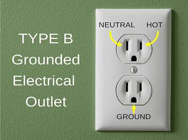
Figure 1: A 110-volt power outlet in the U.S.
Since the neutral and ground wires go to the same place, they are electrically interchangeable. In fact, if they were electrically shorted at the outlet with a single wire connection back to the service box, it would be difficult to detect any difference. So why run two wires instead of one? The simple answer is that ground and current return are two separate functions that are not usually compatible. Significant currents flowing in a conductor can prevent it from being a reliable reference potential.
The most important point to make about grounding for safety and EMC is that ground is not a current return path. Ground and current return are both very important concepts, but they are not the same thing. Ground is NOT a path for returning currents to their source. Ground is the zero-volt reference for product circuits and systems. The concept of ground plays a critical role in design for safety and design for electromagnetic compatibility.
Grounding for Safety
An important part of designing safe electrical products and systems is knowing where and when unsafe voltages may appear on various conducting surfaces. From a safety perspective, ground is the zero-volt reference. For buildings, the ground reference is usually the earth under the building (or literally the “ground” beneath the building). This is convenient, because the earth is large and all large metal structures (e.g., plumbing and cables that penetrate the boundary of the building) are easily connected or referenced to earth ground.
Building grounds are typically metal rods driven into the dirt near the power service entrance. These rods are connected to the breaker box from which ground is distributed to all power outlets through non-current-carrying wires. They are also connected to any metal that is distributed throughout the building, such as plumbing pipes or building steel.
Appliances or electrical products with a substantial exposed metal surface are typically required to ground the metal to the earth ground wire to ensure that it cannot reach an unsafe potential relative to any other grounded metal in the building. If a fault occurs that causes a short between a power conductor and the exposed metal, the ground connection to the breaker box ensures that a large amount of current is drawn. This forces the circuit breaker to open and removes power from the appliance.
Safety ground conductors must be capable of carrying fault currents long enough to blow a fuse or trip a circuit breaker. They cannot carry intentional power currents when an unsafe voltage backs those currents.
It’s important to note that this method of ensuring that products are safe relies on a good connection from the power outlet ground to the breaker box. Older power outlets may be missing a ground terminal, and even new outlets that are improperly wired may be missing the ground connection. For this reason, many products employ designs that do not rely on the ground connection for safe operation. Double-insulated products are designed to ensure that the power connection cannot short to exposed metal, either by eliminating exposed metal and/or ensuring that the circuit breaker will be tripped if any shorting occurs.
There are also a growing number of electrical products with embedded ground-fault circuit interrupter (GFCI) devices. GFCIs operate by sensing when there is a current imbalance between the power-in and power-return wires, as illustrated in Figure 8.2. At the first sign of a current imbalance exceeding a safe threshold, the GFCI disconnects the power.
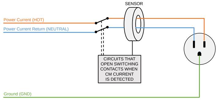
Figure 2: Diagram illustrating the basic operation of a GFCI.
Safety grounds may or may not be the same as EMC grounds, but grounding for safety can be an important factor to consider when designing for EMC. For example, in medical products and industrial controls, circuit grounds are often required to be isolated from chassis grounds for safety reasons. This presents a unique design challenge to EMC engineers, who want to see all large metal objects well-connected at high frequencies.
Grounding for EMC
EMC problems are often the result of two large metal objects at different potentials. At high frequencies, potential differences of just a few hundred microvolts between two resonant conductors can cause a product to exceed radiated emissions limits. Similarly, voltage differences induced between two conductors that are not well-connected can result in radiated immunity problems.
Grounding involves defining a zero-volt reference and bonding metal objects or circuits to that reference through a low-impedance, non-current-carrying connection. A proper EMC grounding strategy ensures that large metal structures cannot be driven relative to each other, resulting in unintended emissions or immunity problems. Bonding metal objects to keep them at the same potential and referencing all external connections to the same zero-volt ground is a key step to ensuring the electromagnetic compatibility of most products.
Ground Structures
Nearly all electronic devices and systems have a ground structure. In buildings, it’s the ground wires, plumbing and metal structure. In cars and aircraft, it’s the metal frame or chassis. In most computers, it’s the metal support structure and/or enclosure.
The ground structure serves as the local zero-volt reference. Anything large and metal should not be allowed to take on a potential significantly different from the ground structure. This is generally accomplished by bonding all large metal objects to the ground structure at the frequencies of interest. It can also be accomplished by sufficiently isolating large metal objects and ensuring that there is no source that can cause a potential to develop between them.
For example, consider the satellite shown in Figure 8.3. Its ground structure is the metal enclosure that houses most of the electronics. In order to couple any significant electromagnetic power into or out of the satellite, it would be necessary to establish a voltage difference between the ground structure and something else of significant electrical size. At frequencies below a few hundred megahertz, the only conductors of significant electrical size (other than the ground structure) are the two solar panel arrays and possibly any wires connecting these arrays to circuits inside the satellite.
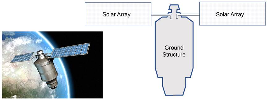
Figure 3: Satellite with two solar arrays.
Bonding the solar panel arrays to the enclosure at the points where they are in close proximity ensures that significant voltage differences will not appear between large conductors that can serve as unintentional transmitting or receiving antennas for noise. Connecting wires would also need to be bonded to the ground structure. This would generally be accomplished through shunt capacitors, in order to establish a bond at noise frequencies while allowing power and signal currents to flow unattenuated.
This grounding strategy is not only important for meeting radiated emissions and immunity requirements, but it also plays a key role in meeting conducted emissions and immunity requirements where the ground structure is both the zero-volt reference and the preferred path for potentially interfering noise currents.
Three important points to make about ground structures are,
- The ground structure must be a good conductor at the frequencies of interest, but it does not have to be electrically small. Occasionally, you may hear someone make the argument that ground doesn’t exist at high frequencies because ground is an equipotential surface, and the potential at two points a quarter wavelength apart on a surface is not the same. This argument is unfounded because ground structures are not necessarily equipotential surfaces in that sense. In fact, the whole concept of a uniquely definable potential difference between two distant points falls apart at high frequencies.
The earth serves as a safety ground for most power distribution systems, even though the earth is certainly not electrically small at 50 or 60 Hz. It doesn’t matter that the earth’s potential in Los Angeles is not the same as it is in New York. Ground structures do not need to be electrically small. - The ground structure does not have to enclose the electronics. A ground structure is not a shielding enclosure. It is simply something large and metallic that serves as a local zero-volt reference for anything else that is large and metallic.
- The ground structure cannot carry intentional currents (at least not at the amplitudes and frequencies of interest). Currents flowing on or in a conductor cause magnetic flux to wrap the conductor. Magnetic flux wrapping a conductor induces a voltage across it. At high frequencies, this voltage difference can potentially drive one part of the ground structure relative to another part.
Ground structures may carry currents at frequencies and amplitudes that do not impact their effectiveness as a ground structure. For example, most automobiles utilize the vehicle frame as the return current path for lights and non-critical sensors operating at very low frequencies. This does not degrade the frame’s ability to serve as a ground structure at higher frequencies.
It is important to note that while the ground structure cannot carry intentional currents, it is expected to carry fault currents and induced noise currents. In fact, the proper utilization of the ground structure depends on its ability to carry unintentional currents with a sufficiently low impedance to control unintentional voltage differences.
Grounding Conductors
Grounding conductors are the connections (e.g., screws, bolts, gaskets, wires or metal straps) that bond large metal objects to the ground structure. Like ground structures, grounding conductors do not carry intentional currents. Their function is to keep the voltage difference between the two metal structures below a critical value.
Grounding conductors must have a sufficiently low impedance (i.e., resistance plus inductive reactance) to ensure that their impedance times the maximum fault current they might carry is below the minimum voltage difference that could result in an EMC problem. For example, suppose the shield of a shielded twisted wire pair is connected to the ground structure through a 1-cm connector pin, as illustrated in Figure 4. The twisted wire pair carries a 100 Mbps pseudo-differential signal with a common-mode noise current of 0.3 mA at 100 MHz. The voltage driving the cable shield relative to the board is approximately equal to the current returning in the shield times the effective inductance of the shield connection. Assuming the effective inductance of the connector pin is approximately 10 nH (i.e., 1 nH/mm), the voltage driving the cable shield relative to the ground structure is approximately 2 millivolts. In many situations, this is sufficient to exceed the radiated emissions limit at 100 MHz, and steps would need to be taken to reduce the common-mode noise or reduce the connection inductance of the grounding conductor.
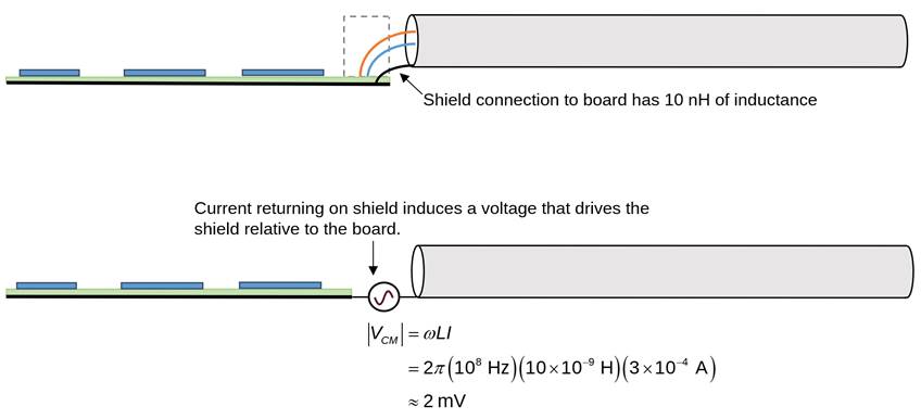
Figure 4: Twisted pair with shield connected to ground structure.
Galvanic Corrosion
When a grounding connection is made by bolting two flat metal surfaces together, the resistance of the connection can be more important than the inductance. This is particularly true when the interface between them becomes corroded.
Galvanic corrosion potential is a measure of how quickly dissimilar metals will corrode when they are in contact. Corrosion depends on the presence of an electrolyte, such as water, and the rate of corrosion depends on many factors, including the properties of the electrolyte.
The chart in Figure 5 lists the anodic index for several common metals next to their names. This parameter is a measure of the electrochemical voltage that will develop between the metal and gold. To find the relative voltage of a pair of metals, their anodic indices are subtracted, as indicated in the chart. Depending on the environment, bonds between materials with a voltage difference greater than 0.95 volts generally require plating or gaskets to preserve the integrity of the bond over time.
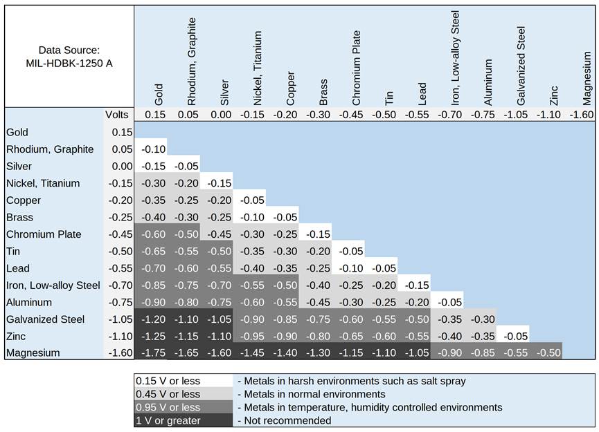
Figure 5: Anodic indices for common metals.
Ground vs. Current Return
As indicated at the start of this chapter, ground and current return are two very different functions. Unfortunately, many current-return conductors are labeled “ground” in real products. This creates a great deal of confusion as rules related to ground get applied to current returns and vice versa.
For example, the partial board schematic in Figure 6 has four different grounds. One component works with signals or power that reference three of these grounds. It’s very unlikely that the designer of this circuit wanted four different zero-volt references. In fact, the four grounds are connected by jumpers, indicating that the designer intended to have one zero-volt reference.
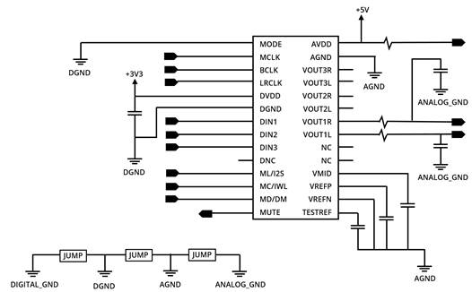
Figure 6: Partial schematic with four grounds.
The board layout shown in Figure 7 shows a layer with two isolated nets labeled “GND” and “AGND”. Isolating grounds makes it difficult to keep all the large metal objects in a system at the same potential. Generally, it should only be done when necessary for safety reasons. So why are these “grounds” isolated?
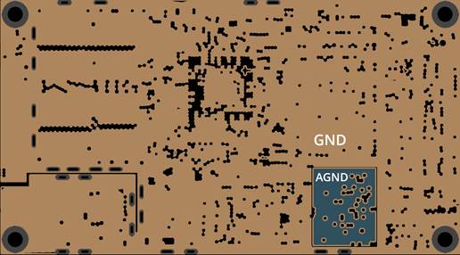
Figure 7: One layer of a board layout with two grounds.
In the two examples above, the reason the “ground” nets were isolated is that they were not really grounds. They were the return conductors for power or signal currents. The designers didn’t want isolated zero-volt references. They were attempting to isolate current return conductors to avoid common-impedance coupling.
About 50 years ago, when digital circuits were just beginning to make their way into products such as radios and high-fidelity audio equipment, it became clear that digital noise could be coupled to the audio circuits when they shared the same current return conductors. For example, consider the simple board illustrated in Figure 8.8a. It has two digital components, a digital-to-analog (D/A) converter, and an amplifier to boost the analog signal before it is sent off the board through a connector. A single-ended digital signal between the two digital components uses a solid copper plane as a return path. At kilohertz frequencies and below, the current returning on the plane spreads out with a distribution approximately represented by the orange lines in Figure 8b. The low-frequency current returning from the amplifier to the D/A converter follows a path approximately represented by the blue lines in Figure 8b
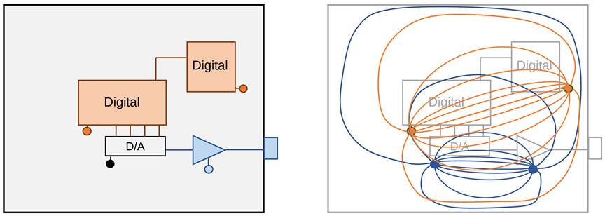
Figure 8: A simple mixed-signal board on the left (a) and the approximate return current distribution on the current return plane (b).
There is clearly a great deal of overlap in the current distribution. This results in common-impedance coupling because the currents in one circuit share a return plane resistance with the currents in the other circuit. If the shared return plane resistance were on the order of 1 mW, and the digital currents were on the order of 100 mA, then the voltage difference induced in the analog circuits would be on the order of 100 mV.
Fifty years ago, engineers designing audio circuitry observed that the voltage difference induced in audio circuits due to common-impedance coupling from the digital circuits was often unacceptable. People could hear digital noise in the acoustic signal. The solution was to isolate the digital signal return currents from the analog signal return currents. Boards with more than two layers were not common back then, so a popular approach was to gap the current return plane. An example of this is shown in Figure 9.
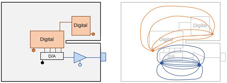
Figure 9: A mixed-signal board with a gap in the current return plane on the left and the approximate return current distribution on the current return plane.
Since low-frequency currents cannot flow across a gap, the currents are redirected on either side of the gap. This reduces the digital return current density in the region of the plane used primarily by the analog currents and reduces the common-impedance coupling.
On the relatively simple two-layer boards of the 1960s and 1970s, gapping the “ground” plane between analog and digital circuits was often an effective way to eliminate unacceptable crosstalk due to common impedance coupling. Unfortunately, it worked so well that people eventually got the idea that current return planes should always be gapped between digital and analog circuits. A design rule was born, and board designers love design rules. Fifty years later, many board designers still adhere to this design rule even though it no longer makes sense. In fact, a better design rule for today’s boards is to never gap the current return plane between analog and digital circuits.
To illustrate why this is so, consider the board layout in Figure 10. It has the same components as the previous example and, like the previous example, it gaps the current return plane between the analog and digital circuits. However, in this case, the gap surrounds the analog circuit on three sides.
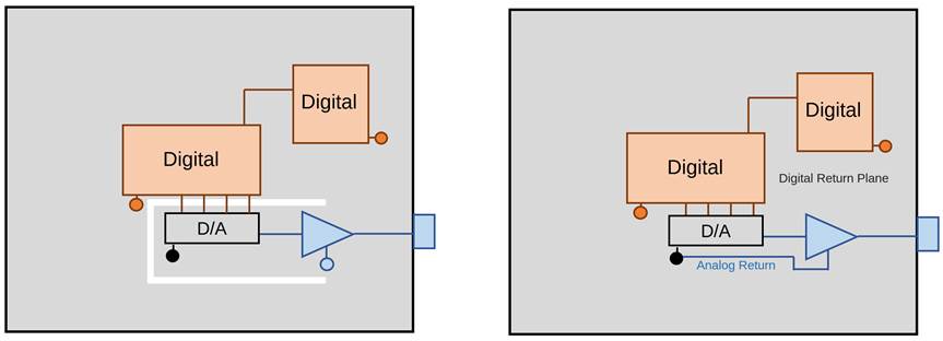
Figure 10: A terrible mixed signal board layout on the left and a much better alternative layout on the right.
Plotting the return currents, as was done in the previous example, would illustrate excellent isolation between the digital and analog return currents. But the previous return current plots did not account for all the currents in the plane. Note that there are four digital traces connecting the D/A converter to one of the digital components. These signals also require return currents. Those currents must get from the D/A component’s ground pin to the digital component’s ground pin. This path was short and inconsequential before, but now the gap forces these currents to share the same region of the plane as the analog currents. Instead of making things better, this gap potentially makes things much worse.
Properly locating the gap between the analog and digital circuits is critical. It was often difficult to determine the right location for the gap fifty years ago. In today’s high-density boards, gapping the planes is generally an unworkable and completely unnecessary solution to a non-existent problem.
There are at least three reasons why gapping a current return plane is not necessary with today’s board designs:
- Digital and analog signals tend to operate at much higher frequencies than they did 50 years ago. At frequencies above about 100 kHz, the return currents on a plane are confined to the regions directly below the signal traces. Since they don’t spread out on the plane, gapping the plane doesn’t improve the isolation between the circuits.
- At kHz frequencies and lower, the resistance of circuit board return planes is less than 1 mW/square. This means that “noisy” circuits dumping amperes of current into the plane are only capable of inducing millivolts (worst case) of voltage difference in other circuits sharing the same plane. There are not many situations where this level of noise coupling is likely to be a problem.
- In those situations where a milliohm of coupling cannot be tolerated, it is much better to isolate one of the returns on a different layer. For example, the best solution to the coupling problem in our previous example was not to gap the plane. Figure 8.10b demonstrates how returning the analog current using a trace on the top layer avoids the common impedance coupling problem. In boards that have lots of analog and digital returns that must be isolated at low frequencies, it is usually necessary to connect them at high frequencies to prevent radiated emissions problems. Routing isolated returns on adjacent layers makes it much easier to establish a good high-frequency connection between them.
Notice that the analog current return trace in Figure 10b is connected to the digital current return plane with a single via located near the D/A ground pin. The via does not carry significant analog or digital return currents. Its sole function is to ensure that the analog and digital circuits have the same zero-volt reference. In other words, the via is a grounding conductor, whereas the plane and the trace are current-return conductors.
Single-point and Multi-point Grounds
Suppose the analog current-return trace in Figure 10b had two via connections to the digital current-return plane, as shown in Figure 11. Now the analog return current has two possible paths. It can return on the trace, or it can return on the plane. At low frequencies, the current will split according to the resistance of each path, permitting significant amounts of analog current to return on the plane. Likewise, some digital current will flow on the analog current return trace. The isolation is destroyed, and the common-impedance coupling is reintroduced.
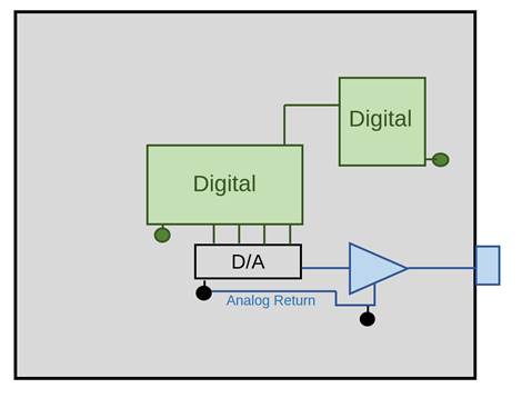
Figure 11: Adding a second connection between two isolated current returns can mean they are no longer isolated at low frequencies.
Generally speaking, two current-return paths are not isolated at low frequencies if they are connected at more than one point. The via connection in Figure 10b is an example of a single-point ground. Single-point grounding is an important concept in EMC, though it is often misunderstood by designers who have not properly made the distinction between current-return and grounding conductors.
Figure 12 illustrates the single-point grounding concept. Isolated circuits or systems are tied to a single point through non-current-carrying grounding conductors. Figure 13 shows another implementation where the grounding conductors connect at more than one point, but they are all still referenced to a single point. One example of this is the power ground in buildings. Every grounded device has a dedicated wired path to the building's electrical service. Still, parallel paths are created by plumbing connections or products whose external metal surfaces are in electrical contact. Connecting the grounding conductors at more than one point does not diminish the effectiveness of the grounding scheme.
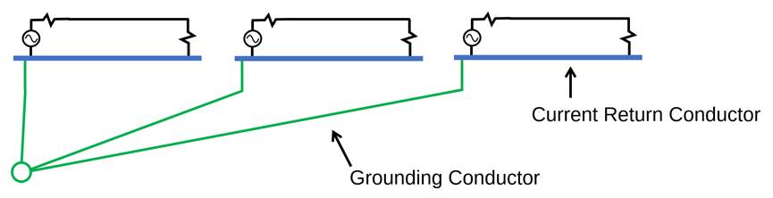
Figure 12: A single-point ground.
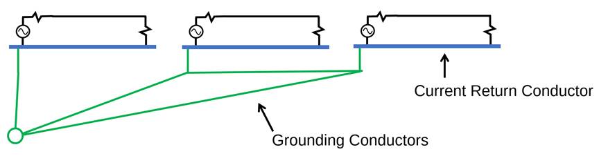
Figure 13: Another single-point ground implementation.
While single-point grounding is an important concept for ensuring that isolated circuits have the same zero-volt reference, it doesn’t work if the grounding conductors carry signal or power currents. For example, in Figure 14, the middle and right-hand circuits are not isolated. Currents returning from the load to the source of the middle circuit now have the option of returning through the intended blue conductor or traveling over the additional connection to the right-hand circuit and back to the middle circuit through the “single point” ground.
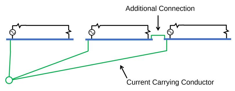
Figure 14: This is NOT a single-point ground.
The path in Figure 14 from the single-point connection to the middle circuit to the right-hand circuit and back to the single-point connection is sometimes referred to as a ground loop. Ground loops are often considered to be inconsistent with single-point grounding and often cited as the source of common impedance coupling, but this is incorrect. Figure 13 has a ground loop, and it’s still a good single-point ground implementation. The ground loop in Figure 14 includes a segment that is not ground at all. The blue conductor in the middle circuit may be called a “ground” in the board layout, but it is a current-return conductor.
Generally, ground loops are fine if all the conductors in the loop are really ground conductors. If one or more conductors in the loop are low-frequency current-return conductors, then all the conductors in the loop will carry a portion of that return current. This can facilitate common-impedance coupling.
Figure 15 illustrates another example of a misapplication of the single-point ground concept. This example was drawn from a manufacturer’s application note advising customers how to lay out a three-phase motor driver. The idea was to ensure that all three phases had the same zero-volt reference as the motor. The implementation called for returning all the switching currents and the motor current to the same point.
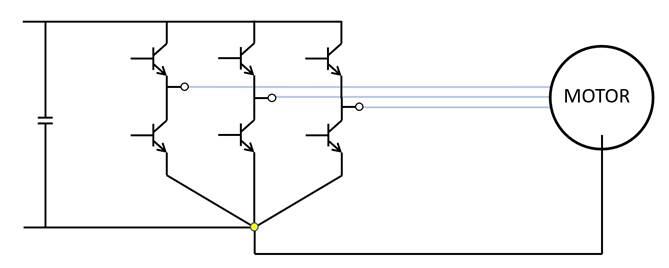
Figure 15: A single-point current-return (bad idea).
Of course, this is not a single-point ground. Although all the conductors are labeled ground on the schematic and in the board layout, they are not grounds. They are current-return conductors.
Sending all the switching currents to a single point in the layout basically ensures that the inductance of the connection will be higher than it would be otherwise. It ensures that there will be a high common impedance as well as a mutual inductance between phases. It also ensures that none of the phases or the motor will have the same zero-volt reference.
Basically, it’s important to remember that single-point grounding is a strategy for ensuring that isolated circuits and devices have the same zero-volt reference. Single-point current returns, on the other hand, are often the root cause of EM coupling problems.
The alternative to a single-point grounding strategy is a multipoint grounding strategy. An example of this is illustrated in Figure 16. Instead of a single point, ground is defined locally. This is essentially the ground structure concept described earlier.
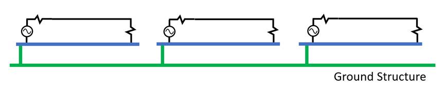
Figure 16: A multipoint ground.
It is common for systems employing a ground structure to connect circuits and modules that are not isolated to the ground structure at more than one point. A simple example of this is illustrated in Figure 17.
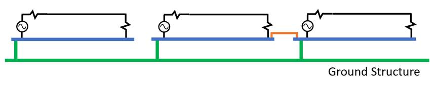
Figure 17: A hybrid grounding strategy.
In this case, the connection between the middle and right-hand circuits allows low-frequency return currents to flow on the ground structure. So, at low frequencies, the structure may not be a reliable ground and would more correctly be described as a current-return structure.
When coming up with a grounding strategy, it’s important to realize that a conductive structure can serve a grounding function at some frequencies and a current-return function at others. For example, in automotive systems, low-frequency communications and DC power distribution typically utilize the frame of the vehicle as a current return. This reduces the weight and improves the reliability of the vehicle electronics. At low frequencies (DC-kHz), the frame is not a ground structure; it is a current-return structure. At high frequencies (MHz and higher), the frame serves as a multipoint ground structure.
This hybrid grounding strategy works well for many non-automotive products as well. Hybrid grounds are commonly employed in home appliances, consumer electronics, computers, telecommunication equipment, and industrial controls. However, some industries (notably aerospace and medical electronics) may prohibit the flow of low-frequency power or signal currents on the chassis. For these products, the hybrid grounding strategy in Figure 17 is not an option. Single-point or multipoint grounding can be employed, or circuits may be completely isolated from the ground structure. These products still require a high-frequency connection between large metal objects and the ground structure if those objects might otherwise acquire a significant voltage relative to the structure.
Circuit Board Ground
When laying out a circuit board, it’s important to identify and utilize the board’s EMC ground. The EMC ground serves as the local zero-volt reference for everything big and metal attached to the board, including power and signal wires.
If the circuit board is mounted in a plastic enclosure with no system-level ground structure nearby, the PCB EMC ground will be the area of the board’s current return plane that is under or near an external connector. Care must be taken to ensure that no signals are routed parallel to the connector so that the entire area has a common reference potential. An example of this is illustrated on the left side of Figure 18.
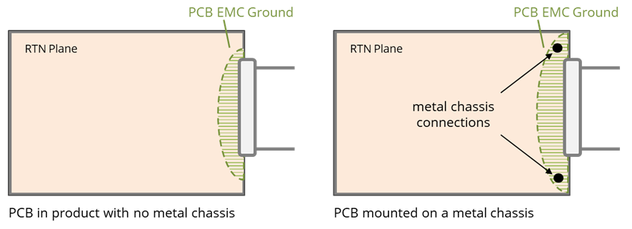
Figure 18: Location of the EMC ground on circuit boards with and without a metal chassis.
If the board is mounted on or near a metal chassis, it’s important to connect the PCB EMC ground to the chassis. This helps to prevent the board from driving an attached cable relative to the chassis ground. Connection points should be located on both sides of the connector to minimize the inductance of the chassis connection.
If the board is mounted to a solid metal chassis at several locations, it’s possible to have a PCB EMC ground at each location, as illustrated in Figure 19. This is important when the board has more than one connector, and it’s not possible to locate all connectors on the same edge of the board.
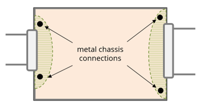
Figure 19: PCB chassis connections when connectors are on more than one edge.
If the board is not mounted to a metal chassis, all external connections should be made to one edge of the board. High-speed circuitry located between external connections tends to drive one cable relative to another. If there is no metal chassis to hold the cables to the same potential, this can result in radiated emissions problems. Mounting connectors to opposite sides of a board with no metal chassis can also facilitate immunity problems by pulling induced currents across the board.
References
[1] American National Standard Dictionary for Technologies of Electromagnetic Compatibility (EMC), Electromagnetic Pulse (EMP), and Electrostatic Discharge (ESD), ANSI C63.14-1992.
[2] NFPA 70, National Electrical Code.
[3] IEEE 1050, Guide for Instrumentation and Control Equipment Grounding in Generating Stations, IEEE, 2004.
[4] T. Van Doren, Grounding and Shielding of Electronic Systems, Course Notes, 1983-2009.