Shielding Theory
Ask the average engineer on the street about controlling electromagnetic interference and the response will probably involve shielding. Virtually all high-speed electronic devices employ shielding in some form. Computers, cell phones, video games, industrial controls, automotive and avionic systems, etc., all typically come packaged in metal (or metalized) enclosures or have shields located directly over specific components on their printed circuit boards.
Shielded enclosures that are properly designed and installed can be a very effective means of attenuating radiated emissions and protecting products from external sources of interference. In fact, a metallic enclosure with no apertures, seams or cable penetrations can typically reduce radiated emissions and improve radiated immunity by 40 dB or more. In other words, even a poorly designed circuit board can meet EMC requirements if it is sealed in a metal box.
However, shielded enclosures are a poor substitute for good EMC design at the board level. Effective enclosures can add significant cost and weight to a product and a single breach of the enclosure (e.g. an unfiltered cable penetration) can completely eliminate any benefit the enclosure would otherwise provide. In many cases, a product in a poorly designed shielded enclosure will radiate more (or be more susceptible) than the same product without the enclosure.
Shields work by reflecting, absorbing or redirecting electric and/or magnetic fields. It is not always necessary for a shield to completely enclose a product in order to be effective. For example, partial shields are often utilized to redirect fields on or above a source circuit to isolate it from another circuit or to prevent coupling to cables or other unintentional antennas.
Choosing proper location, orientation and material for a shield requires a knowledge of the type of field being shielded and the objectives of the shield. The following sections will describe basic shielding theory and provide several examples of good shielding in various situations.
Plane-Wave Shielding Theory
When an electromagnetic wave propagating in one material encounters another material with different electrical properties, some of the energy in the wave is reflected and the rest is transmitted into the new material. For example, consider the electromagnetic plane wave, Einc, incident upon an infinite slab of material as illustrated in Figure 1. The wave propagates in free space in the x direction until it strikes the material, which has intrinsic impedance, ηs.
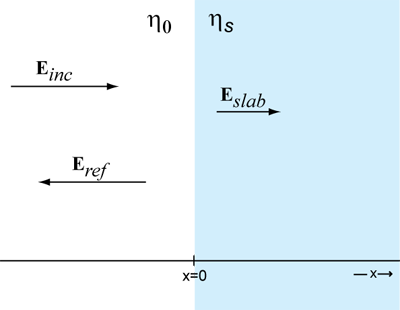
Figure 1: Plane wave incident on a shielding material
The magnetic field in the plane wave is perpendicular to the electric field and has amplitude,
(1)
where is the intrinsic impedance of free space (~377 ohms).
When the plane wave strikes the slab, a reflected wave, Eref, and a transmitted wave, Eslab, are created. The magnetic field in the shielding material is related to the electric field,
(2)
In addition, the boundary conditions on the surface at x=0 require that,
(3)
and
(4)
where the subscripts x=0- and x=0+ indicate the fields, just to the right or left of the x=0 surface. In order to satisfy Equations (1) through (4), the amplitude of the reflected field must satisfy the relation,
(5)
where ΓE is the electric field reflection coefficient,
(6)
The amplitude of the transmitted field, Eslab, is
(7)
where
(8)
is the electric field transmission coefficient.
Note that as ηs gets closer to η0, the transmission coefficient increases, and the reflection coefficient decreases. If ηs = η0, all of the incident field is transmitted.
If the material in Figure 1 is lossy, (i.e., σ≠0), the transmitted wave will decrease in amplitude as it propagates,
(9)
where δ is the skin depth of the material. For high-loss materials,
(10)
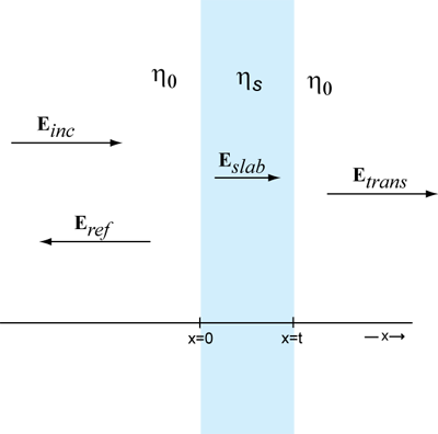
Figure 2: Plane wave incident on a finite thickness shielding material
Now consider the finite slab of shielding material illustrated in Figure 2. An incident field, Einc, strikes the surface of the shielding material. Some of the power in the field is reflected and some continues into the material. The part that penetrates into the material is attenuated before it strikes the second surface at x=t. At that point, once again some of the power is attenuated and some of the power is transmitted. If the attenuation is high, the power reflected at the second interface is absorbed and the field transmitted to the region of free space on the right of the slab is given by,
(11)
where
(12)
Combining (7), (8), (9), (11) and (12); we obtain an expression for the transmitted electric field in terms of the incident field,
(13)
This expression applies to any shield material that is much thicker than a skin depth. Typically, the best plane-wave shields will be good conductors with a high conductivity,  . For good conductors,
(14)
For these materials,  and Equation (13) reduces to,
(15)
If we define the shielding effectiveness of the slab to be,
(16)
then the shielding effectiveness of an infinite sheet of good conductor can be written in the form,
(17)
where the total shielding effectiveness is observed to consist of two terms. The reflection loss, R(dB), is the attenuation due to the reflection of power at the interfaces. The absorption loss, A(dB), is the attenuation due to power converted to heat as the wave propagates through the material. A web-based calculator for determining the plane-wave shielding effectiveness of various materials can be found here.
The reflection loss is independent of the thickness of the shield and depends entirely on the mismatch between the shield's intrinsic impedance and the intrinsic impedance of free space. The absorption loss is directly proportional to the thickness of the shield expressed in skin depths,
(18)
Example 1: Calculating Shielding Effectiveness of Copper Foil
Calculate the shielding effectiveness of a sheet of 2-mil copper foil, σ = 5.7x10⁷ S/m, at 100 MHz.
We start by calculating the skin depth in copper at 100 MHz,
(19)
The material thickness (t = 2 mils = 50.8 μm) is clearly much greater than the skin depth so (17) can be used to calculate the shielding effectiveness. In fact, the absorption loss can be easily calculated as,
(20)
To calculate the reflection loss, we need to determine the intrinsic impedance of copper at 100 MHz,
(21)
Then the reflection loss is quickly determined to be,
(22)
The overall shielding effectiveness is the sum of the reflection loss and the absorption loss,
(23)
Note that virtually all of the incident power is reflected by the shield. 154 decibels is a very large ratio, suggesting that the transmitted power is smaller than the incident power by a factor of 1015. In practice, attenuations of this magnitude are neither realizable nor measurable. The largest realizable field strengths (without causing ionization of the air) are on the order of 106 V/m. The smallest detectable field strengths (using sensitive field probes) are on the order of 10-6 V/m. This represents a possible dynamic range of,
(24)
As a practical matter, most engineering test equipment has a maximum dynamic range of around 80 - 120 dB. Therefore, any calculated attenuation or shielding effectiveness much higher than 100 dB implies the material is essentially impenetrable. A material with a calculated shielding effectiveness of 154 dB is essentially no better or worse than a material with a calculated value of 120 dB.
If the material in Fig. 2 is not thick relative to a skin depth, some of the energy that reflects off the second interface (at x=t) propagates back into the slab and is reflected off the inside of the first interface (at x=0+). This energy will then again strike the second interface and some fraction will be transmitted adding to the total energy transmitted and reducing the shielding effectiveness. The wave may bounce back and forth multiple times before attenuating to the point where it no longer contributes significantly to the transmitted field. If the absorption loss term in (17) is less than about 15 dB, the accuracy of the shielding effectiveness estimate is compromised by these multiple reflections.
For conductive materials that are electrically thin (i.e., t<<λ), we can adjust the expression for shielding effectiveness (17) by adding a third term to account for multiple reflections resulting in a general expression for plane-wave shielding effectiveness [1, 2],
(25)
Note that the multiple reflection loss term has a negative value and reduces the overall shielding effectiveness for thin materials. This term provides an indication of when the high-loss assumption used to derive (17) has been violated. If the multiple reflection loss factor is comparable to the reflection loss, then the shielding effectiveness approximation in (17) is not accurate.
Near-Field Shielding
Plane-wave shielding theory conveniently permits us to calculate a shielding effectiveness value for any shielding material based on its material properties and thickness. Unfortunately, practical shields are never located in the far-field of both the source and receptor circuits. Because of this, we are very unlikely to have plane wave propagation on both sides of the material and the calculated shielding effectiveness will not correspond to anything we are likely to measure (except in specially designed test fixtures).
In order to help understand how near-field shielding differs from plane-wave shielding, consider the configurations shown in Figure 3. In Figure 3(a), the incident plane wave has been replaced by a small electric dipole source and the shielding material is located in the near field of the source. In Figure 3(b), the source is a magnetic dipole, represented by a small loop of electric current.
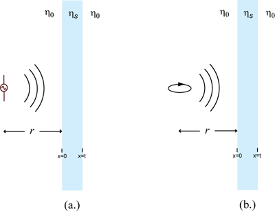
Figure 3: Shielding electric and magnetic dipole sources.
Recall that in the near field (r << λ), an electric dipole source has a strong electric field. The wave impedance in the near field is approximately,
(26)
In the near field of a magnetic dipole source, the magnetic field dominates and the wave impedance is approximately,
. (27)
We can estimate the shielding effectiveness of the slab in Fig. 3, by substituting the wave impedance ( ) for the intrinsic impedance of free space, η0, in (25). This yields a new expression for the reflection loss term,
. (28)
The expressions for absorption loss and multiple reflection loss are unchanged. Although this type of shielding effectiveness calculation is a simple approximation that does not correspond to any particular realizable test structure, it can provide a great deal of insight relative to the performance of various shielding materials in realistic situations. There is a near-field shielding effectiveness calculator based on these equations on the web at,
Plane Wave Shielding Effectiveness Calculator (select the "Near-Field Approximation" radio button).
Example 2: Shielding a Low-Frequency Magnetic Field Source
A transformer generating primarily a magnetic field is located 10 cm from a shielding structure. The shielding structure is made from a 1-cm thick sheet of copper. Estimate the shielding effectiveness of this structure at 1.5 kHz.
If we start by modeling the transformer as a magnetic dipole source, we can quickly estimate the wave impedance at the position of the shield to be,
. (29)
The intrinsic impedance and skin depth of the copper are,
(30)
. (31)
The calculated shielding effectiveness is therefore,
. (32)
Note that in this case the absorption loss plays an important role in the overall shielding effectiveness. Generally, at low frequencies close to a magnetic field source, the wave impedance is low and therefore the reflection loss due to conductive shields is less significant. Absorption loss also decreases as frequencies get lower, but not as quickly as reflection loss.
Shielding Effectiveness Measurements
Plane-wave shielding effectiveness
As discussed in the previous section, the concept of plane-wave shielding effectiveness is convenient because it is a function of only the material properties and thickness of a shielding material. Attempts to measure the plane-wave shielding effectiveness generally involve launching a guided TEM wave in a coaxial test fixture containing a sample of the material, as illustrated in Fig. 4.
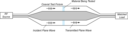
Figure 4. Shielding Effectiveness Test Fixture
The transmission line structure has a specific characteristic impedance (usually 50 ohms). The cross-sectional dimensions are scaled up in the mid-section of the test fixture in order to accommodate a reasonably sized material sample, which is disk-shaped with a hole in the center. The measured shielding effectiveness is simply calculated as,
termination.(33)
When measurements are made with a network analyzer, the shielding effectiveness can be conveniently express in terms of the s-parameters as,
. (34)
Note that even though the characteristic impedance (ratio of of the test fixture is 50 ohms, the ratio of |E| to |H| is still determined by the intrinsic impedance of the medium ( ohms in air).
Other shielding effectiveness measurements
Of course, the effectiveness of a shielded enclosure may be very different from the plane-wave shielding effectiveness of the material from which the enclosure is made. Many factors influence the effectiveness of a shielded enclosure including the size and shape of the enclosure and the type and location of the source. Also, typically power escaping through apertures and seams in a real enclosure is much more significant than any power propagating directly through the enclosure walls.
For this reason, it is usually more practical to define the shielding effectiveness of an enclosure as follows,
. (35)
For example, suppose the measured radiated field from an electronic product was measured with no enclosure (or a plastic enclosure) and found to be 52 dB(μV/m). Then suppose that the same product was tested in exactly the same manner with a metallic enclosure and the measured field strength was 38 dB(μV/m). The shielding effectiveness of the enclosure in this particular configuration would then be reported as,
(36)
This is probably a much lower value than the plane-wave shielding effectiveness, but it accounts for the leakage through apertures and seams. It also takes into account the fact that shielded enclosures generally interact with the enclosed sources and the enclosure itself becomes an integral part of the unintentional antenna path converting currents into radiated fields.
Quiz Question
The shielding effectiveness of an enclosure made of a material that has a plane-wave shielding effectiveness of 60 dB is,
- ~60 dB
- always less than 60 dB
- usually greater than 60 dB
- sometimes less than 0 dB
Recalling the previous discussion of unintentional radiation sources and antenna efficiency, it should be clear that an inefficient radiation source (e.g., an electrically small circuit) can become many orders of magnitude more efficient by coupling to a larger conducting structure. Therefore, it is not only possible, but common, for a shielding enclosure with apertures or seams to increase the radiated emissions due to inefficient sources enclosed. In other words, the shielding effectiveness of a shielded enclosure can easily be less than 0 dB (i.e., the enclosure amplifies the radiation) at some frequencies. Hopefully, the same enclosure also reduces the efficiency of the strongest sources so that the net effect is a reduction in the maximum radiated emissions. Nevertheless, it is not safe to assume that some shielding is better than no shielding. A discussion of practical shielding techniques for solving real-world EMC problems can be found in the tutorial on Practical Shielding.
References
[1] H. Ott, Electromagnetic Compatibility Engineering, John Wiley & Sons, New York, 2009.
[2] C. R. Paul, Introduction to Electromagnetic Compatibility, 2nd Ed., Wiley Series in Microwave and Optical Engineering, 2006.