Not-So-Good EMC Design Guidelines
These design guidelines are either too vague, do not apply often enough to be useful, or are just wrong.
Circuit Board Layout
A ground plane should completely fill the area under every component without voids, except where necessary for via holes.
This is generally a good idea, but there are many situations where it is not a good idea to bring the ground plane under a component or a particular area of the board (e.g. some transformers, chokes or power supply circuits). Blindly following this guideline can result in significant EMC problems.
On multi-layer boards, the best stack-up is ....
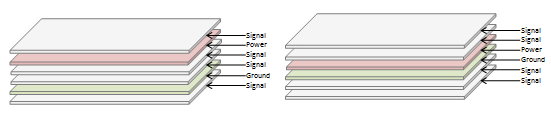 S-S-P-G-S-S? S-P-S-S-G-S? The truth is there is no guideline for the optimum layer stack-up that applies to more than a small subset of all boards. The optimum layer assignments depend on many factors. Any attempt to determine layer assignments based on a general guideline is unlikely to produce an optimum design. In fact, rigidly assigning an entire layer to any particular type of circuit trace is generally not a good idea.
Above 25 MHz, all boards should have two ground planes.
This is apparently a very old guideline. These days many perfectly good boards operate at GHz frequencies with only one ground plane. The number of ground planes required depends on many factors (e.g. the number of nets and the total number of layers). The frequency of the fastest circuits should not be the deciding factor.
On boards with multiple ground planes, use ground vias around the perimeter of the PCB every 2 cm to form a Faraday cage.
On most boards with two or more ground planes, there are enough naturally occurring via connections to make this guideline unnecessary. On boards that don't have enough naturally occurring via connections, placing the vias around the outer edge of the board will create a resonant cavity. In this case, it is better to distribute these connections throughout the board rather than placing them all near the edge.
There should be no floating metal of any kind near any PCB.
While generally this is a true statement, attempting to ground every single piece of metal on a board no matter how insignificantly small can actually make a design worse. It is important to use good judgment and determine whether a small piece of floating metal (e.g. an electrically small heatsink or a small patch of copper on a board) is really worth the effort to ground. A poor grounding attempt can add to the electrical size of the floating metal and create a problem that would not have otherwise existed.
A solid ground "island" should be placed under all large ICs.
Ground islands in general are a bad idea (e.g. see gapping a ground plane under The Worst EMC Design Guidelines). If the ground island is on a layer above or below a solid ground plane, it might serve a useful purpose in some rare situations, but this should not be on anyone's list of "general" EMC design guidelines.
For PCBs without a ground plane, a minimum of one ground-return track should be routed adjacent to each eight lines of address and data lines. For the address lines, route the ground return next to the least significant bit (LSB) since this line is likely to be the most active.
This might be just what is required for some boards, but not all boards (not even most boards). The number of ground traces and their placement can be a critical design parameter in a board without ground planes. This decision should never be made based on a design guideline.
High-frequency, low-inductance ceramic capacitors should be used for integrated circuit (IC) decoupling at each power pin. Use 0.1 µF for up to 15 MHz, and 0.01 µF over 15 MHz. The decoupling capacitor should be located as close as physically possible to the IC’s power pin.
The guidelines for decoupling are strongly dependent on the spacing between the power and ground planes (or whether there is a power plane at all). General guidelines regarding the size and placement of decoupling capacitors are dangerous, because they can result in very poorly decoupled boards when they are applied in the wrong situation.
Use the lowest power, slowest logic that satisfies circuit requirements.
Not a bad idea, but relying on the slowness of a logic family to control your risetimes is dangerous. Unless you're using logic with a controlled slew rate, any logic family you choose is likely to become faster over time. IC suppliers routinely make improvements to their products that shorten the transition times. A product that relies on slow logic to control risetimes may no longer meet its EMC requirements when it starts being manufactured with the "improved" components.
Nets driven at faster than 1V/ns slew rate must have a discrete series resistor at the source.
Whether or not you need to add a discrete resistor at the source depends many things, but (generally speaking) the slew rate is not one of them.
Capacitively-loaded nets must have a total source impedance equal to or greater than one-quarter of the line characteristic impedance or a series resistor must be added to meet this condition.
This is not one of them either. In fact, this is never one of them.
Guard traces should be used to isolate high-speed nets from I/O nets.
Guard traces are not useless, but they are not useful often enough to warrant a mention in anybody's list of design guidelines. We recommend that you not use guard traces unless there is a specific known problem you are trying to address.
All power and ground traces must be at least three times the nominal signal line width.
Not a bad sentiment, but not always necessary or sufficient.
Additional decoupling capacitors should be placed on both sides of a power or ground plane gap.
Ground Plane Gap?!! Don't gap the ground plane! Gap the power plane all you want, but we can't think of any compelling reason to put additional decoupling on both sides of the gap. This was probably conceived as a method for reducing coupling between two power bus structures, but the decoupling capacitors are unlikely to be effective at the frequencies where this type of coupling is likely to be a problem.
Daughter boards (with high-frequency devices and/or external cables) must be properly grounded to the motherboard and/or chassis (do not rely on the ground pins in the connector to provide this ground).
This is good advice, except when it is bad advice. Don't confuse current return paths with grounds. We generally want signal currents to return on the connector pins. Each situation is unique and overly general guidelines like this can cause designers to do exactly the wrong thing in a given product.
Critical nets should be routed in a daisy chain fashion with no stubs or branches.
Sometimes, yes. Sometimes, no.
Cards and enclosures should be designed so that their resonances do not match harmonics of system clock frequencies.
Theoretically, this is a good idea. In practice, it is not reasonable to expect that a designer controls all the parameters that affect the resonant frequencies of cards or enclosures. Attempts to do so waste resources and may compromise the integrity of the design.
Switch-mode power supply traces should be routed on one layer of the circuit board with the ground plane directly on an adjacent layer to minimize the loop area.
Minimizing loop areas is generally a good idea, but this guideline can be misleading. The key focuses of a switch-mode power supply layout should be the switching voltage node and the switching current loop. Routing all traces on the same layer may yield the best layout. Also, supplies generating 100 Watts or more may require an isolated return for the switching currents. Like many of the guidelines in the "not-so-good" category, this may be the right thing to do sometimes, but not every time.
Shielding
A shield must completely enclose the electronics eliminating any penetrations such as holes, seams, slots, or cables.
Guidelines like this generally fail to indicate that there are four categories of shielding: Electric-field shielding, LF magnetic-field shielding, HF magnetic-field shielding and shielded enclosures. The guideline above would only apply to shielded enclosures. Holes, seams, slots and cable penetrations are usually an essential element of any practical enclosure. Eliminating them is not an option, so this guideline is not particularly helpful. Also, most shields in commercial products are electric-field shields. These shields can be effective, even with holes, seams, slots and wire penetrations.
Each shield must have a low-impedance contact to ground in at least two places in order to prevent its noise potential from coupling to the enclosed object.
If you have more than one shield in your product, they are probably electric-field shields. The location where electric-field shields are grounded is critical. Advising engineers to "ground them in at least two places" is terrible advice.