Power Bus Decoupling Guidelines for Printed Circuit Boards with Widely Spaced Power Distribution Planes
Applicable to:
Multi-layer boards with power distribution planes spaced more than 0.5 mm apart
Introduction
-
In boards with widely-spaced power distribution planes, the inductance due to the loop area between the planes cannot be neglected. In fact, this inductance can be used to enhance the board's power bus decoupling.
-
Local decoupling capacitors on boards with widely spaced planes can effectively reduce noise on the power bus at frequencies up to several GHz if they are mounted properly.
-
The mutual inductance between closely spaced vias can force current to be drawn from a nearby decoupling capacitor before it is drawn from the power distribution planes [1-3].
-
In order to take advantage of this phenomenon, it is important that the connection inductance of the local decoupling capacitors is minimized. It is also important to locate these capacitors very close to the device being decoupled.
General Guidelines
-
Multi-layer boards generally employ two types of decoupling capacitor. Large-valued "bulk" capacitors help to minimize the impedance of the power bus at low frequencies (e.g. below a few hundred kHz). These are "global" decoupling capacitors that respond to the current needs of all active devices on the board. Smaller "high-frequency" capacitors reduce the power bus impedance at higher frequencies. When properly mounted, these are "local" decoupling capacitors that primarily provide current to one active device.
-
Boards typically have one or two large electrolytic bulk decoupling capacitors or they may employ half a dozen or more bulk decoupling capacitors in smaller packages. Either approach is effective and this decision is normally made based on size, cost and board-area constraints.
-
The total value of the bulk decoupling is determined by the transient power requirements of the active devices on the board. Generally, the total bulk decoupling capacitance is 1 - 10 times the total high-frequency decoupling capacitance connected to the power bus.
-
Local decoupling capacitors are intended to be effective at higher frequencies. The inductance of their connection to the power distribution planes is far more critical than their nominal capacitance. Generally, smaller package sizes can be connected to the planes with a lower inductance than larger packages. Therefore, local decoupling capacitors should generally be as small (physically) as possible.
-
Choose the largest nominal capacitance available in a given package size. Nominal capacitance values are not nearly as critical as connection inductance. Typically, local decoupling capacitors on boards with widely spaced planes have a nominal value of about 0.01 microfarads.
-
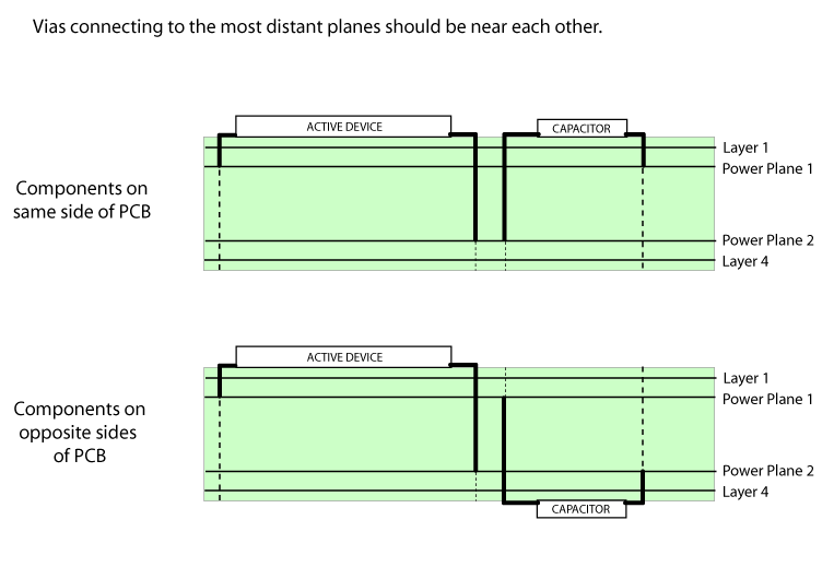
The location of the local decoupling capacitors is critical. Local decoupling capacitors should be located as close as possible to the power or ground pins of the active device they are decoupling. To determine near which pin to locate the decoupling capacitor (e.g. Vcc, Vss, Vdd, GND), first determine which power distribution plane is furthest from the active device. Local decoupling should be provided near the pins that connect to the most distant plane. For example, if the components are above Layer 1 on a 4-layer board and Layers 2 and 3 are Vcc and GND respectively, then the decoupling capacitors should be located near the GND pins of the active device. If there are any active devices below Layer 4 on this board, then decoupling for these devices should be located next to the Vcc pins.
-
Orient the local decoupling capacitor so that the pin connected to the most distant plane is nearest the active device's pin connecting to the most distant plane. For example, in the examples below if the active device is above Layer 1, and the decoupling capacitor is below Layer 4, then the Vcc pin of the decoupling capacitor should be located near the GND pin of the active device. Decoupling capacitors should never share a via with an active device when they are located on opposite sides of the board.
-
If the decoupling capacitor can be located near enough to the active device to share the same via, this is optimal. However under no circumstances should a trace be used between the decoupling capacitor mounting pads and the vias. Decoupling capacitors should have vias located in or adjacent to the mounting pads to minimize their connection inductance. To minimize connection inductance:
-
Never use traces on decoupling capacitors! Locate the via adjacent to the mounting pad.
-
Locate the two capacitor vias as close together as possible.
-
Mount all of the local decoupling capacitors on the face of the board closest to the planes. Connection inductance is nearly proportional to the distance from the planes.
-
Examples
The figure below shows two examples of good local decoupling capacitor connections to boards with widely spaced power distribution planes.
References
[1] T. H. Hubing, T. P. Van Doren, F. Sha, J. L. Drewniak, and M. Wilhelm, "An Experimental Investigation of 4-Layer Printed Circuit Board Decoupling," Proceedings of the 1995 IEEE International Symposium on Electromagnetic Compatibility, Atlanta, GA, August 1995, pp. 308-312.
[2] J. Fan, J. Drewniak, J. Knighten, N. Smith, A. Orlandi, T. Van Doren, T. Hubing and R. DuBroff, "Quantifying SMT Decoupling Capacitor Placement in DC Power-Bus Design for Multilayer PCBs," IEEE Trans. on Electromagnetic Compatibility, vol. EMC-43, no. 4, November 2001, pp. 588-599.
[3] J. Fan, W. Cui, J. Drewniak, T. Van Doren, J. Knighten, "Estimating the Noise Mitigation Effect of Local Decoupling in Printed Circuit Boards," IEEE Trans. on Advanced Packaging, vol. 25, no. 2, May 2002, pp. 154-165.