EMC Question of the Week: April 6, 2026
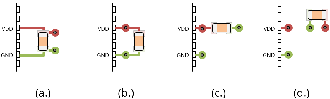
An IC that is internally clocked at 1 GHz is mounted on an 8-layer printed circuit board. Board layers 2, 4, and 7 are GND planes. Layer 5 is a VDD plane. The IC has 6 VDD pins. The figure illustrates four possible ways to connect the decoupling capacitors. Which connection scheme is best for this IC on this board?
Answer
The best layout option is (d.) Since the VDD plane is on a layer next to a GND plane, minimizing the connection inductance to the planes is the priority. The connections to the planes in (d.) have the lowest inductance and will supply the most current to the IC at high frequencies.
Option (a.) is the worst option at high frequencies because it puts significant inductance in the GND connection to the IC. This limits the ability of the IC to get charge quickly and introduces unnecessary "ground bounce" (i.e., a spiking voltage difference between the PCB and IC ground references). Connections between a high-speed IC (or a capacitor) to the ground plane should generally go directly to the plane without an intervening trace.
Option (b.) allows the IC and the decoupling capacitor to share a single via connection to the GND plane. If there is a GND plane on the layer directly below the components, this is not a terrible option, but it is not the lowest inductance connection. This option and option (a.) also make trace routing more difficult because they partially block access to some of the component pins on Layer 1.
Option (c.) would have been the best option if the VDD and GND planes were not on adjacent layers. In that situation, local decoupling capacitors should generally share the via that connects to the most distant power plane. However, there is no advantage to doing this when VDD and GND are on adjacent layers.
Option (d.) minimizes the connection inductance between the IC and the planes as well as the connection inductance between the decoupling capacitor and the planes. The VDD and GND vias are located as close to each other as possible without any significant trace length between the via and solder pad. The capacitor is located a little farther from the IC, but that will not have any measurable effect on the power bus impedance as observed by the IC.
Note: Given the short traces and close proximity of the capacitors in the first three configurations. None of them are actually that bad. In each case, the connection inductance is comparable to the inductance in the lead frame of the IC. An important point here is that (d.) not only works slightly better than the other three, it's also more convenient. It's easily implemented and leaves more room for other traces connecting to the IC. Another important consideration is that the first three options only work well when the distance from the capacitor to the IC is comparable to the vertical distance from the board surface to the plane pair. Option (d.) does not have this limitation.
Have a comment or question regarding this solution? We'd like to hear from you. Email us at