EMC Question of the Week: June 19, 2017
At frequencies above 1 MHz, gapping the current-return plane in a printed circuit board is an effective way to reduce,
- electric-field coupling
- magnetic-field coupling
- common-impedance coupling
- all of the above
- none of the above
Answer
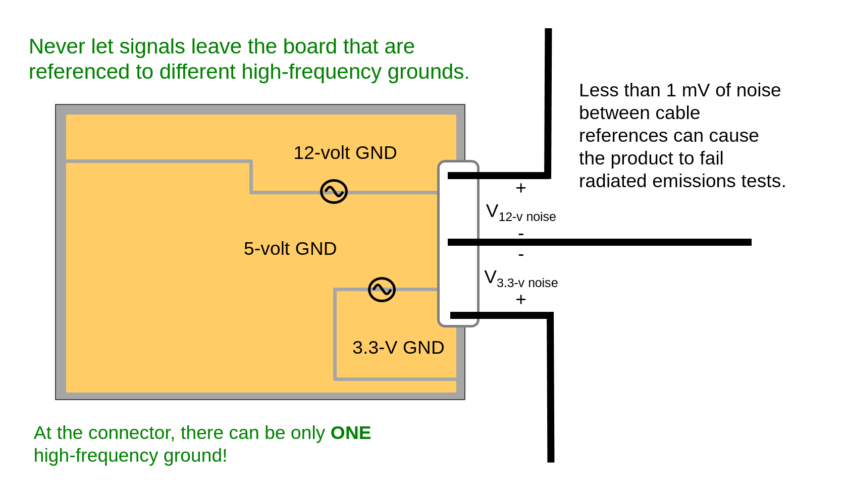
The correct answer is "e. none of the above". Gapping a solid current-return plane in a printed circuit board is almost always a bad idea. Gapping a solid current-return plane promotes differences in the reference voltages of various circuits. At high frequencies, this can cause radiated emissions and immunity problems.
Above 1 MHz, currents will return directly below their corresponding signal traces, so common-impedance coupling can be avoided by routing signal traces above their own portion of a solid return plane. It is also important to realize that above 1 MHz, common-impedance coupling is unlikely to be the dominant coupling mechanism. For two signal traces side by side over a solid return plane, gapping the plane between them can actually increase the electric-field and magnetic-field coupling.
In board designs that have a genuine need to isolate low-frequency return currents, it is generally better to route these return currents on different layers. This provides effective low-frequency isolation while making it easier to reconnect them at high-frequencies where field coupling is much more likely to be an issue.
Have a comment or question regarding this solution? We'd like to hear from you. Email us at