Basic Transmission Lines
Electrical signals propagate in circuits with a finite velocity. In many cases, the time delays associated with signal propagation are negligible. However, for signals with high-frequency content that propagate significant distances, these delays cannot be ignored. Transmission line modeling is a relatively simple and intuitive way to analyze circuits with signals propagating on circuit board traces or cables whose length cannot be neglected.

Consider the simple circuit shown in Figure 1 that models a load resistance connected to a source and switch through a pair of wires. The switch closes at t = 0. Applying circuit theory, we expect the voltage across the resistor to change from 0 to VS at time t = 0. However, in real circuits, there is always a delay between the time the switch closes and the time the voltage at the load changes. This is because electromagnetic energy travels with a finite velocity.
In high-speed digital circuit designs, there are many situations where the time delay cannot be neglected. Depending on the properties of the dielectric in which the waves travel, the delay associated with circuit board traces or cables is typically on the order of 35-70 picoseconds per centimeter. A signal traveling across a large circuit board or a short cable may arrive several nanoseconds after it was initially sent.
Beyond the obvious timing implications for digital signals, there is an issue related to the fact that the source cannot initially supply the correct current before it has “seen” the load impedance. As a result, signal energy may bounce back and forth between the source and load before reaching the correct steady-state value. This can result in both signal integrity and electromagnetic compatibility problems.
In situations where the non-zero time delay is significant, engineers can predict and control its effects using uniform transmission line theory. Uniform transmission lines are conductor pairs with a uniform cross-section that carry electrical power or signals. Several common uniform transmission line configurations are shown in Figure 2.
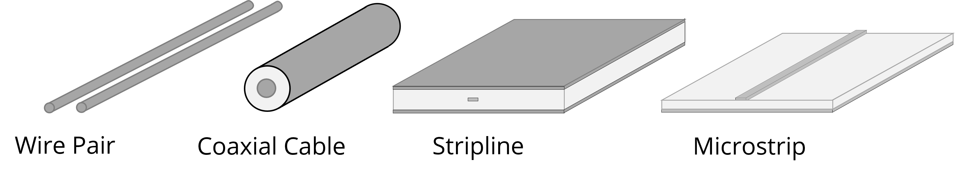
The cross-sectional dimensions of uniform transmission lines must be small relative to the minimum wavelength contained in the signal. However, the length of a transmission line is unconstrained, and practical transmission lines can be hundreds of wavelengths long. Cross-country power lines, telephone wires, TV cables, and high-speed printed circuit board traces are all examples of transmission lines.
In schematics, transmission lines are typically represented by two parallel rectangles, as shown in Figure 3. The symbol resembles a pair of parallel wires, but it is used for any two-conductor transmission line, including microstrip traces and coaxial cables. If the transmission line is short and the propagation delay is negligible, it may not have any properties that need to be included in the circuit analysis. For longer conductor pairs, transmission line models can be combined with traditional circuit models to characterize the circuit's behavior.

Transmission line models recognize that the two conductors have physical properties that may impact their electrical behavior. For example, unless the conductors are superconducting, they will each have a certain amount of resistance. This resistance is not located at a particular point in the circuit but is distributed along the length of the transmission line. The total resistance of the wires is directly proportional to the length of the line. The distributed resistance of the transmission line is the sum of each conductor’s per-unit-length resistance and can be expressed in units of ohms per meter (Ω/m).
Current flowing in the conductor pair sets up a magnetic flux in the space surrounding the conductors. Any change in the current amplitude changes the magnetic flux, resulting in a voltage drop along the length of the line. This voltage can be expressed in terms of an inductance times the rate of change of the current, just as in circuit theory. The inductance is not located at one point. It is distributed along the length of the transmission line and can be expressed in units of henries per meter (H/m).
Transmission lines also have a distributed capacitance, expressed in farads per meter (F/m), due to electric-field coupling between the two conductors. If the dielectric material between the conductors is lossy, current leaking from one conductor to the other through the dielectric can be represented by a distributed conductance expressed in siemens per meter (S/m).

The equivalent circuit shown in Figure 4 models the effects of the distributed resistance, inductance, capacitance, and conductance. In this circuit representation, the distributed parameters of the transmission line are modeled using lumped elements. The lumped element model divides the transmission line into several electrically short (e.g., < λ/10) sections. The inductance of each section is represented by an inductor whose value is the inductance per unit length of the transmission line times the length of the section. A series resistor, a capacitor, and a parallel resistor represent the resistance, capacitance, and conductance of each section.
The model in Figure 4 can be used to accurately model the behavior of TEM wave propagation down the transmission line. For TEM wave propagation on a transmission line with two conductors, the currents on the conductors at any cross-sectional location along the line's length are equal and opposite. The series resistors in Figure 4 represent the sum of the resistances of both conductors. The inductors represent the inductance per unit length of the conductor pair. The model does not attempt to assign partial inductances and resistances to each conductor, since this would unnecessarily complicate the model and encourage misuse. It’s important to note that the reference voltage at the load end will always be undefined relative to the reference voltage at the source end if they are at electrically distant points.
Properties of Transmission Lines
There are four properties of transmission lines that essentially determine how they interact with signal sources and loads,
- propagation velocity
- propagation delay
- characteristic impedance
- and attenuation.
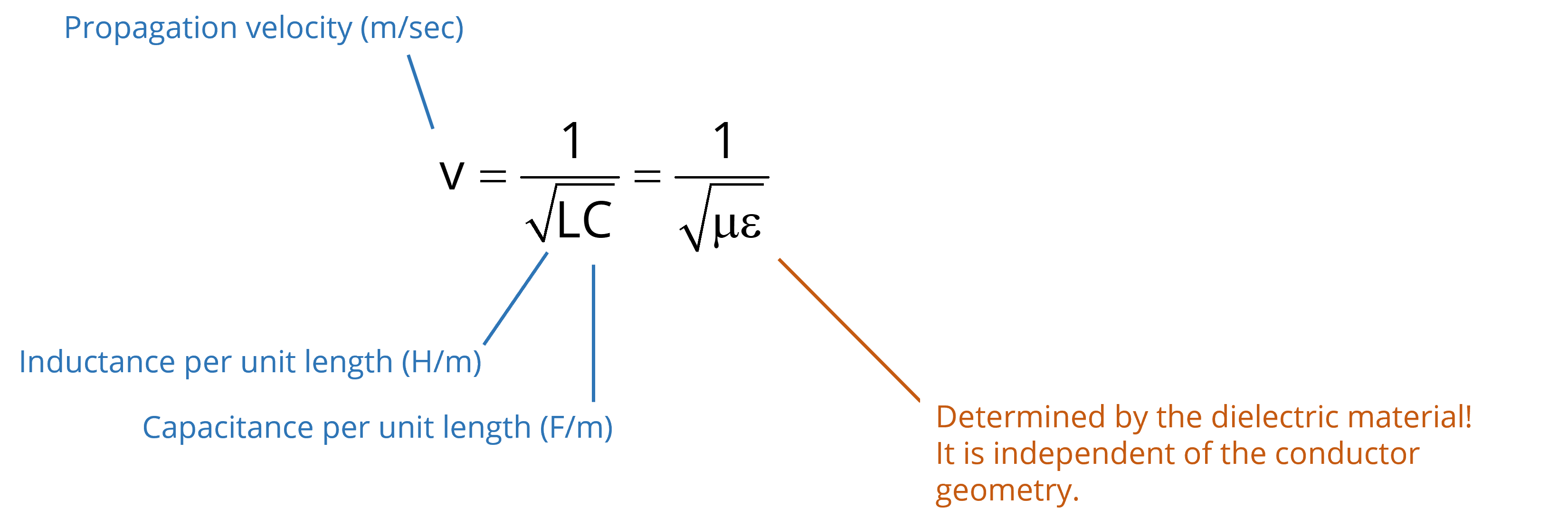
The propagation velocity is the speed at which signal energy moves along the conductor pair. For TEM propagation in low-loss transmission lines, it can be expressed using the equation on the right. Note that the velocity is a function of the inductance per unit length and the capacitance per unit length of the line. However, it can also be expressed as a function of the material properties of the dielectric. The wave energy is carried in the dielectric and guided by the conductors. The velocity of propagation is the speed of light in the dielectric.
It's also worth noting that the product of L and C is a constant for any given dielectric. In other words, any change in the cross-sectional geometry that decreases the inductance will increase the capacitance by the same amount.
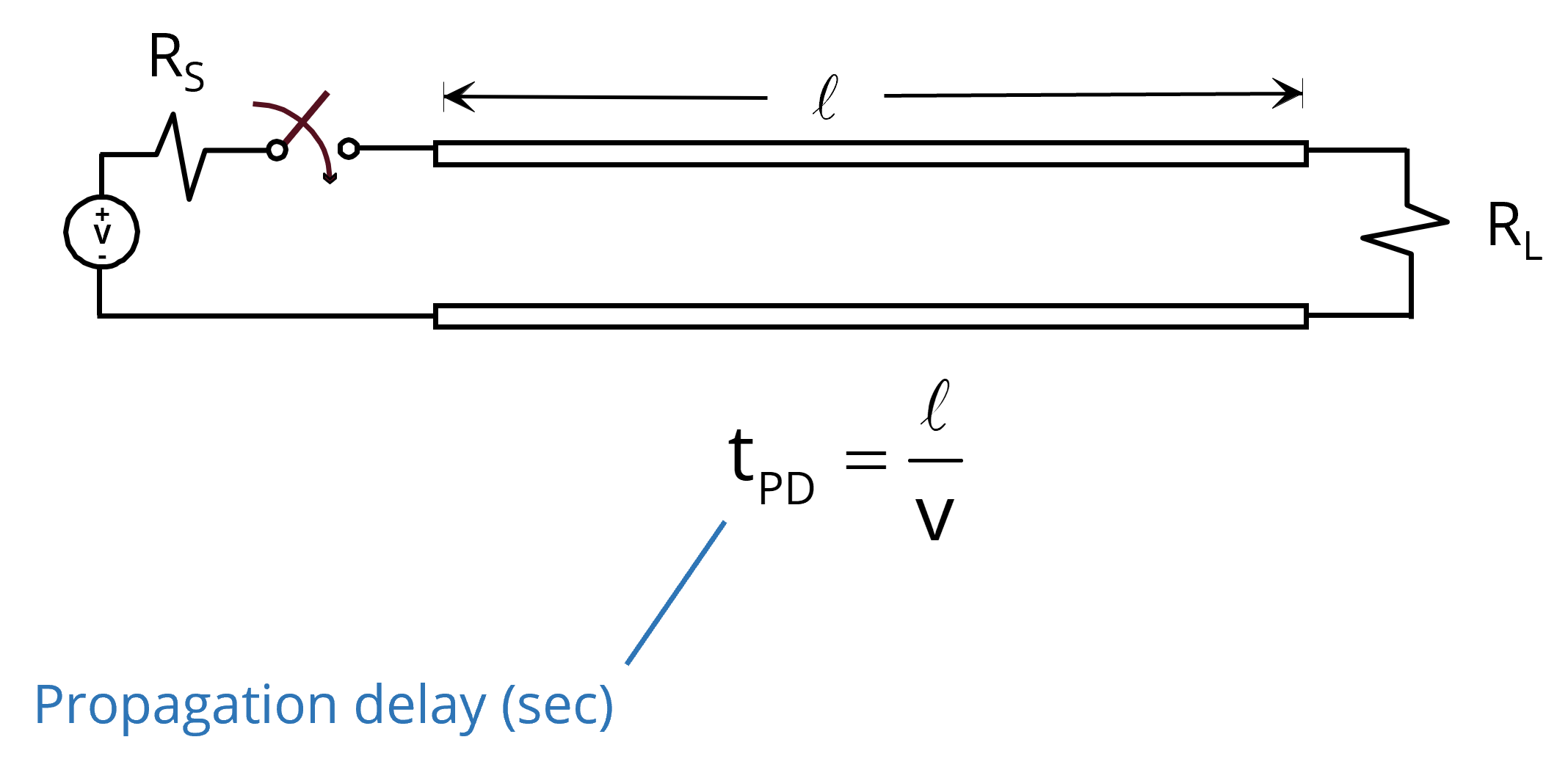
The propagation delay is the time it takes for a signal to move from the source to the load end of the transmission line. It is simply the length of the transmission line divided by the velocity of propagation. The propagation delay is often an important parameter affecting signal integrity. In many situations, it is important to control the delay so that signals arrive at the destination in the correct order. Also, when sending a differential signal as two opposing single-ended signals, it's generally important to ensure that both signals arrive at the destination simultaneously.
Of course, when the switch in Figure 6 first closes, charge immediately begins to flow into the transmission line. The current on each of the two conductors is equal and opposite, but the amount of current initially has nothing to do with the load resistance. Until the signal has had a chance to propagate down to the load and back, the source current depends only on the source resistance and the initial impedance looking into the transmission line. That initial impedance is the characteristic impedance of the transmission line.
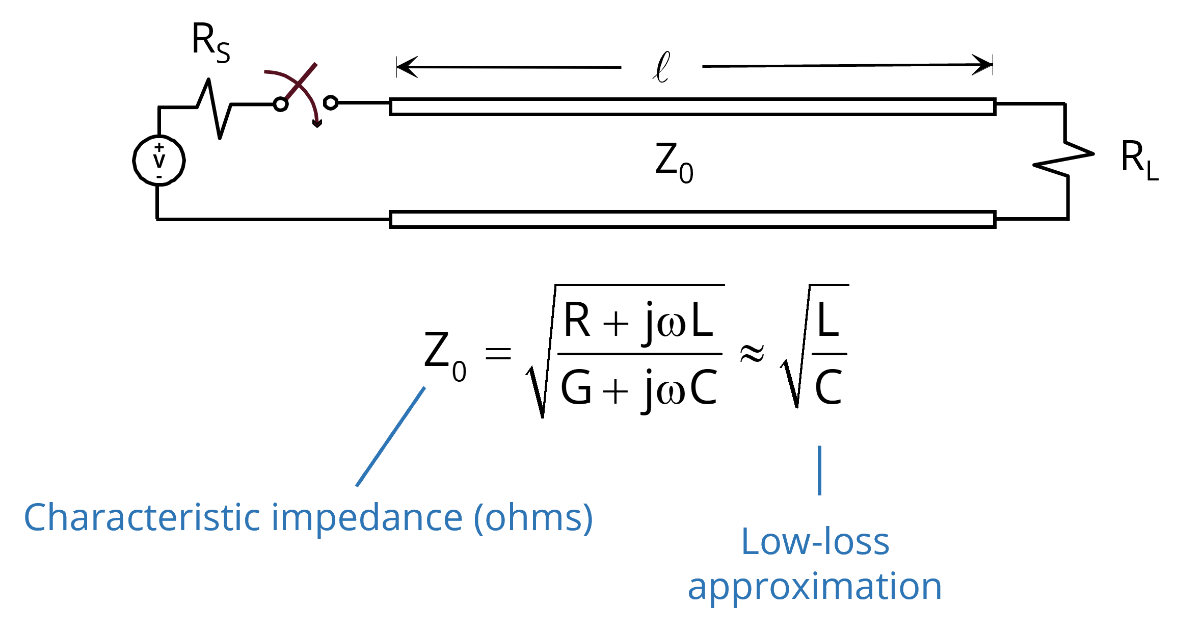
An expression for the characteristic impedance of the transmission line in terms of its RLCG parameters is shown in Figure 7. For most practical transmission lines, it is equal to the square root of the ratio between the inductance and capacitance per unit length.
At the moment the switch closes, the voltage across the transmission line input and the current flowing into the input are the same as they would be if the transmission line were replaced with a resistor that had a value equal to the characteristic impedance, Z0. Except instead of dissipating power as heat, as a resistor would do, the power moves down the line toward the load end.
When the signal reaches the load, if the value of RL is equal to Z0, the ratio of the voltage to the current on the line is correct and power continues to flow toward the load. On the other hand, if RL is not equal to Z0, the ratio of the voltage to the current on the line is not consistent with the ratio that must appear across the load. This inconsistency is resolved by introducing a reflected wave. The voltage and current of the incident wave plus the reflected wave are consistent with the values required across the load. The reflected wave returns to the source end where it encounters the source impedance, RS. If RS is equal to Z0, the circuit has achieved a steady-state voltage and current that are the same values they would have had if the load had been connected directly to the source. If RS is not equal to Z0, another reflection will occur. Waves will continue to reflect back and forth, with each reflected signal being smaller than the previous one, until the reflections are too small to be observed. At that point, the steady-state voltage and current will again be the same values they would have had if the load had been connected directly to the source.
When designing circuits operating at speeds or frequencies where the propagation delay is significant, it is usually necessary to control the characteristic impedance of the connecting wires or traces and provide a termination resistance that is matched to that impedance. For digital signals, this is generally necessary whenever the transition times of the signal are less than twice the propagation delay. For narrowband signals in the frequency domain, this is generally when the length of the connecting wires exceeds about one-eighth of a wavelength.
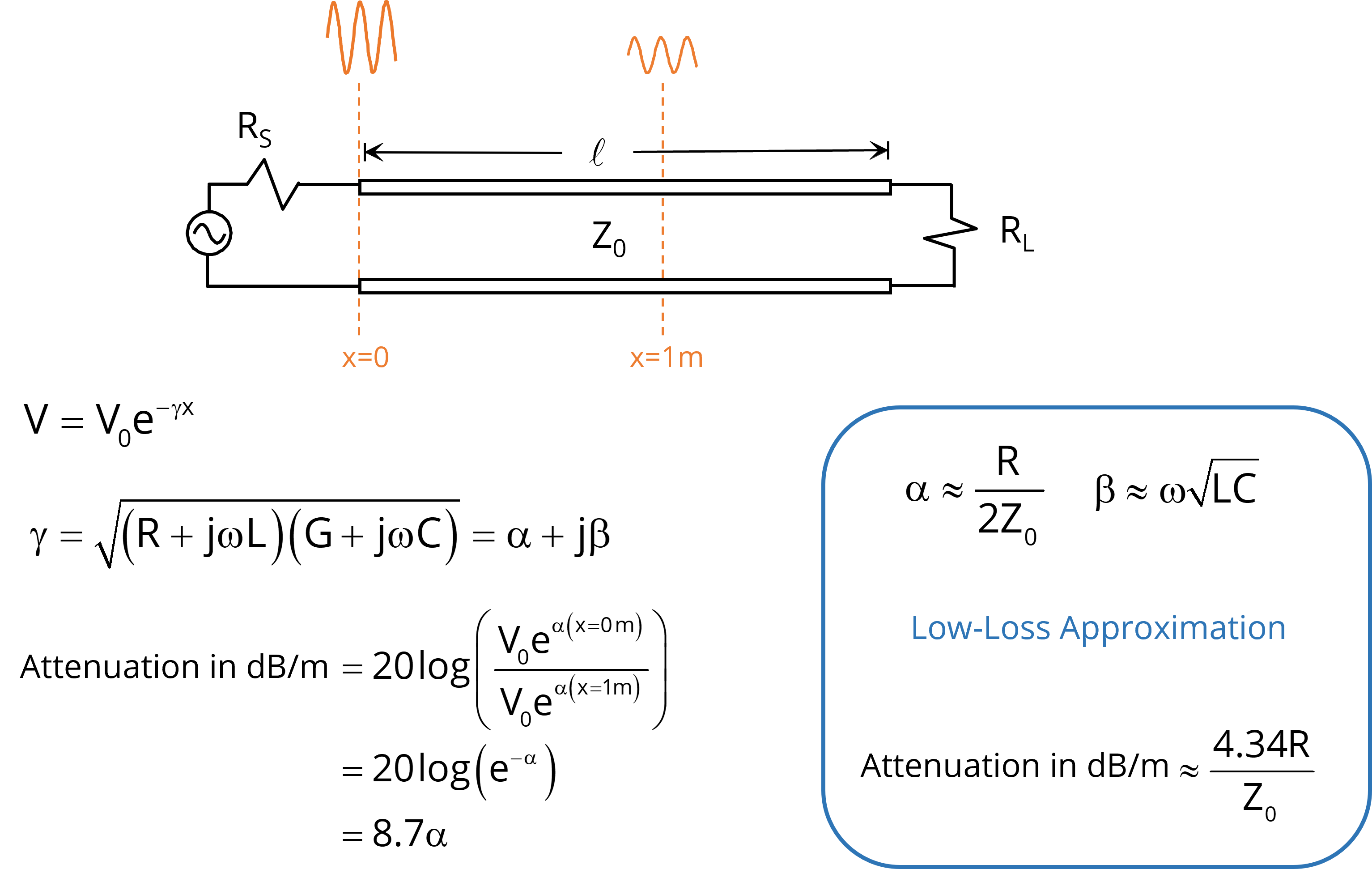
The resistance of the wires or the conductance of the dielectric can generate losses that cause a signal to be attenuated as it propagates down the line. For long lines, the attenuation of the transmission lines can become a signal integrity problem. Frequency-domain equations for the loss in a transmission line are shown in Figure 8.
Generally, loss is expressed as a function of the attenuation constant, α. This constant is a complex function of the conductor and dielectric losses. It is a function of frequency, so time-domain signals may become distorted as they propagate down a lossy line when some of their harmonic components are attenuated more than others.