The Most Important EMC Design Guidelines
Here are four important design guidelines that are often overlooked even though they can be among the easiest to implement early in the design process.
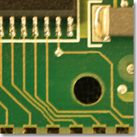
Design Guideline #1: (General) Minimize the Loop Areas Associated with High-Frequency Power and Signal Currents.
This simple rule is on nearly everybody's list of EMC guidelines, but it often gets ignored or compromised in favor of other guidelines. Often the board designer doesn't even know where the signal currents flow. Digital circuit designers like to think of signals in terms of their voltage. Signal integrity and EMC engineers must think of signals in terms of their current.
There are two things that every good circuit designer should know about signal currents.
1. Signal currents always return to their source (i.e. current paths are always loops)
2. Signal currents take the path(s) of least impedance.
At megahertz frequencies and higher, signal current paths are relatively easy to identify. This is because the path of least impedance at high frequencies is generally the path of least inductance, which is generally the path that minimizes the loop area. Currents return as close as possible to the path of the outgoing current. At low frequencies (generally kHz frequencies and below), the path of least impedance tends to be the path(s) of least resistance. Low frequency currents are more difficult to trace, since they will spread out. Significant current return paths may be relatively distant from the outgoing current path.
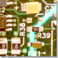
Design Guideline #2: Don't Split, Gap or Cut the Signal Return Plane
Sure, there are some situations where a well-placed gap in the return plane might be called for. However, these situations are relatively rare and always involve a need to control the flow of low-frequency currents. The safest rule-of-thumb is to provide one solid plane for returning all signal currents. In situations where you expect that a particular low-frequency signal is susceptible or is capable of interfering with the circuitry on your board, use a trace on a separate layer to return that current to its source. In general, never split, gap or cut your board's signal return plane. If you are convinced that a gap is necessary to prevent a low-frequency coupling problem, seek advice from an expert. Don't rely on design guidelines or application notes and don't try to implement a scheme that "worked" in someone else's "similar" design.
Design Guideline #3: Don't Locate High-Speed Circuitry Between Connectors
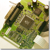
Among board designs that we have reviewed or evaluated in our lab, this is one of the most common problems we've encountered. Many times simple board designs that should have had no trouble at all meeting EMC requirements at no additional cost or effort, wind up being heavily shielded and filtered because they violated this simple rule.
Why is the location of connectors so important? At frequencies below a few hundred megahertz, wavelengths are on the order of a meter or longer. Any possible antennas on the printed circuit board itself tend to be electrically small and therefore inefficient. However, cables or other devices connected to a board can serve as relatively efficient antennas.
Signal currents flowing on traces and returning through solid planes result in small voltage differences between any two points on the plane. These voltage differences are generally proportional to the current flowing in the plane. When all connectors are placed along one edge of a board, the voltage between them tends to be negligible. However, high-speed circuitry located between connectors can easily develop potential differences of a few millivolts or greater between the connectors. These voltages can drive currents onto attached cables causing the product to exceed radiated emissions requirements.
Design Guideline #4: Control Signal Transition Times
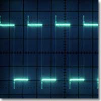
A board operating with a clock speed of 100 MHz should never fail to meet a radiated emissions requirement at 2 GHz. A well-formed digital signal will have a significant amount of power in the lower harmonic frequencies, but not so much power in the upper harmonics. Power in the upper harmonic frequencies is best controlled by slowing the transition times in digital signals. While, excessively long transition times can cause signal integrity and thermal problems, an engineering compromise must be reached between these competing requirements. A transition time that is approximately 20% of a bit period results in a reasonably good-looking waveform, while minimizing problems due to crosstalk and radiated emissions. Depending on the application, transitions times may need to be more or less than 20% of the bit period, however transitions times should not be left to chance.
There are three common methods for controlling rise and fall times in digital logic.
- Use a logic family with a controlled slew-rate.
- Put a resistor or a ferrite in series with a device's output.
- Put a capacitor in parallel with a device's output.
The first choice, controlled slew-rate logic, is often the most effective option, especially when driving a matched termination. However, the majority of the logic circuits on most well-designed boards will have a capacitive termination. Using a series resistor to control the risetime of these circuits gives the designer more control and usually costs less. Ferrites can also be effective, but cost more and provide less control than resistors. Capacitors can actually increase the amount of high-frequency current drawn by the source device and in most cases are not an appropriate choice for transition time control.
Note that it is never a good idea to try to slow down or filter a single-ended signal by impeding the flow of current in the return path. For example, one should never intentionally route a low-speed trace over a gap in a return plane or put a ferrite on a ground in an attempt to filter out the high-frequency noise.