Electromagnetic Radiation
Radiated coupling results when electromagnetic energy is emitted from a source, propagates to the far-field, and induces voltages and currents in another circuit. Unlike common impedance coupling, no conducted path is required. Unlike electric and magnetic field coupling, the victim circuit is not in the electromagnetic near field of the source. Radiated coupling is the only possible coupling mechanism when the source and victim circuits (including all connected conductors) are separated by many wavelengths.
Of the four possible coupling mechanisms, radiation coupling is the one that seems to get the most attention. The idea that currents flowing in one circuit can induce currents in another circuit that is across the room or even miles away is fascinating to most of us. Maxwell's treatise on electromagnetism postulated the existence of electromagnetic waves back in 1864. He was able to calculate the velocity of propagation of these waves, and describe wave reflection and diffraction. However, it was 25 years later before anybody was able to verify the existence of electromagnetic waves. Practical transmitters and receivers were not developed until the beginning of the 20th century. People viewed electromagnetic radiation as something nearly magical. The theory was difficult to comprehend and the equipment required to transmit and receive signals was fairly complicated.
Today, we take wireless communication for granted. It is no longer viewed as magical, but the theory is still complex and the equipment used to send and receive signals is still among the most sophisticated of our time. This leads many engineers to believe that electromagnetic radiation is difficult to create and difficult to detect. However, virtually all circuits radiate and most pick up detectable amounts of ambient electromagnetic fields. It is not necessary to attach an antenna to a circuit to make it radiate, the structure and location of most high frequency circuits allows them to act as their own antenna or to couple to nearby objects that act as efficient antennas.
The more difficult challenge for the designers of most electronic products is to design circuits that don't produce too much electromagnetic radiation. In order to understand how and why circuits exhibit unintentional electromagnetic emissions, it is helpful to review a few general concepts related to electromagnetic radiation and antenna theory.
Fields produced by a time-varying current
Consider the short current filament illustrated in Figure 1. A current with amplitude, I, and angular frequency, ω , extends from . Of course a real current could not start and stop abruptly like this, however realistic current distributions can be modeled by a superposition of current filaments like this one.
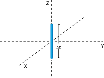
Figure 1. A small current filament.
The magnetic vector potential due to this current can be expressed as,
(1)
where the term represents the delay between the time the current changes at the origin and the time the change can be detected at a point a distance r away. This equation mixes the spherical coordinate r with the Cartesian coordinate z. However, we will avoid this complexity by assuming that the length Δz is small relative to position r and the wavelength, λ . In this case, we can express the magnetic vector potential as,
. (2)
In free space, the magnetic field intensity can be calculated from the magnetic vector potential as,
. (3a)
Note that the magnetic field points in the direction everywhere. It circulates around the axis of the current and has its maximum amplitude in the plane perpendicular to the axis of the current (sin θ = 1). There is no magnetic field on the z axis.
Applying Faraday's Law in point form, we can calculate the electric field as,
. (3b)
The electric field is perpendicular to the magnetic field at every point in space and has both a component and an component.
Although these expressions are fairly complicated, we can appreciate the more important aspects of these field distributions by considering two separate cases: βr << 1 and βr >> 1. The phase constant, β, is inversely proportional to the wavelength, . Therefore, the quantity βr is a measure of how far from the source we are relative to a wavelength,
. (4)
If we are close to the source relative to a wavelength, then βr << 1 and the field terms with (βr)3 in the denominator dominate. This region is referred to as the near field of the source. The near field of the current filament is dominated by the electric field.
When we are far from the source, βr >> 1, the terms with (βr) in the denominator dominate. This is referred to as the far field of the source. If we discard all but the (βr) terms, we get the following expressions for the electric and magnetic far fields,
(5)
and
. (6)
Note that in the far field, E and H are perpendicular to each other and to the direction of propagation, r. The fields are in phase with each other and the ratio of their amplitudes is,
(7)
at all points in space. These are the characteristics of an electromagnetic plane wave. Far from the source, where the spherical wave front is large relative to the size of the observer, the radiated field is essentially a uniform plane wave.
Quiz Question
If the radiated electric field strength 3 meters away from a small source is 40 dB(μV/m), what is the field strength 10 meters away from the same source in free space?
- 40 dB(μV/m)
- 30 dB(μV/m)
- 20 dB(μV/m)
To answer the question above, we note that in the far field of a radiation source, the field strength is inversely proportional to the distance. Therefore, increasing the distance by a factor of 3.3 would reduce the field strength by a factor of 3.3. This is approximately a 10-dB reduction in the field strength, so the correct response would be 30 dB(μV/m).
Fields Produced by a Small Current Loop
Consider the small loop of current illustrated in Figure 2. This current loop can be modeled as 4 current filaments oriented to form a square. We'll let the current amplitude be I0 and the angular frequency be ω as in the previous example. Using the principle of superposition, we can add the electric fields from each current filament to calculate the fields due to the loop. This is a straightforward (though somewhat tedious) process, which is described in many antenna texts. However, for our purposes, the result is more interesting than the derivation, so only the results are presented here.
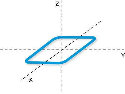
Figure 2. A small current loop.
In free space, the electric field intensity produced by a small loop of current is given by the expression,
(8)
where Δs is the area of the loop. Note the similarity between the electric field produced by the small loop and the magnetic field produced by the current filament (3a). Both point in the direction everywhere. Both are maximum at θ=90°.
Applying Ampere's Law in point form, we can calculate the magnetic field as,
. (9)
The magnetic field from the loop looks a lot like the electric field from the current filament. The magnetic field is perpendicular to the electric field at every point in space and has both a component and an component. If we are close to the source relative to a wavelength (βr << 1) the magnetic field dominates.
When we are far from the source (βr >> 1), we get the following expressions for the electric and magnetic far fields,
(10)
and
. (11)
Again we note that, in the far field, E and H are perpendicular to each other and to the direction of propagation, r. The fields are in phase with each other and the ratio of their amplitudes is η0.
Fields Produced by Electrically Small Circuits
Now let's apply what we know about the radiation from current filaments and current loops to estimate the radiation from an electrically small circuit. We'll start by considering the simple circuit illustrated in Figure 3. This circuit has an ideal voltage source and resistor connected by wire forming a loop with dimensions Δh and Δl. We'll assume that both Δh and Δl are much less than the free-space wavelength, λ.
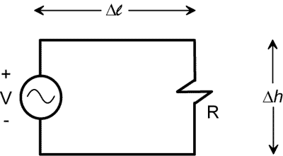
Figure 3. A simple circuit.
If the resistor has a very small value, we might expect this circuit to radiate much like a current loop. The current in the loop would be,
(12)
where LLOOP is the inductance of the rectangular loop. We can plug this expression for the current into Equation (10) to get an expression for the magnitude of the radiated electric field,
. (13)
Since we are normally interested in the maximum radiated field, regardless of orientation, we can replace the sin θ term with its maximum value of 1, resulting in,
. (14)
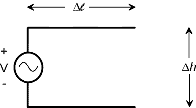
Figure 4. A simple high-impedance circuit.
If R is a high impedance, the circuit does not look like a current loop. However, for very large values of R, we can model the circuit as three current filaments as illustrated in Figure 4. Radiation from the two horizontal current filaments connecting the source to the resistor is relatively low because the currents on these filaments are equal and opposite. However there is a small amount of current flowing in the vertical section of the circuit on the source side. The amount of current flowing in the vertical part of the circuit can be estimated by viewing horizontal filaments as a short length of parallel-wire transmission line. Since the value of R is very large, the impedance at the source end of this transmission line is approximately equal to the input impedance of an open-circuited transmission line,
. (15)
Therefore, the current flowing in the vertical section on the left side of the circuit in Figure 4 is approximately,
. (16)
If we substitute the above equation for I into the equation for calculating the far electric field from a current filament (5), we get
. (17)
We'll simplify this expression by noting that Δh • Δl = Δs and that the characteristic impedance of a parallel wire transmission line, Z0, is typically a few hundred ohms, which is approximately the same as η0. We'll also take the maximum value of the magnitude of this expression as we did for the low-impedance circuit, resulting in the following simple estimate of the maximum radiated field from a high impedance circuit,
. (18)
Note the similarity between the expression for high-impedance circuits (18) and the expression for low-impedance circuits (14). Both are proportional to the source voltage and the loop area. Both are proportional to the square of the frequency and inversely proportional to the distance from the source. The only difference between the two expressions is that the low-impedance circuit expression has an additional η0/ZLOOP term. This suggests a practical method for distinguishing between a high-impedance circuit and a low-impedance circuit and we can estimate the maximum radiated electric field strength from any electrically small circuit using the following expression:
. (19)
Example 1: Estimating the Radiated Field from an Electrically Small Circuit
Calculate the maximum radiated field from the circuit illustrated in Figure 5. Do the emissions from this circuit exceed the FCC Class B limit?
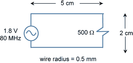
Figure 5. A 500-ohm circuit.
First we need to determine whether or not the circuit is electrically small at the frequency of interest. At 80 MHz, the wavelength in free space is 3.75 meters. Since the maximum dimension of the circuit is much less than a wavelength, we can use Equation (19) to estimate the maximum radiated field from this circuit.
The impedance is 500 ohms, which is greater than the 377-ohm intrinsic impedance of free space, so we use the upper equation in (19),
. (20)
The FCC Class B limit at 80 MHz is 100 μV/m or 40 dB(μV/m), suggesting that this circuit would be 2.5 dB over the limit. However, the field calculated above is in free space and the FCC EMI testing is done in a semi-anechoic environment (above a ground plane). Reflections off the ground plane may add in-phase or out-of-phase with the radiation directly from the circuit. Since we are calculating the maximum radiation (and since the FCC scans the antenna height looking for the maximum), we should double our calculated field strength (i.e. add 6 dB) to account for the presence of the ground plane. In this case, our estimate of the maximum emissions from the circuit above a ground plane becomes 48.5 dB(μV/m) or 8.5 dB above the FCC Class B limit.
As the example above indicates, the presence of a ground plane complicates a radiation calculation. If the ground plane is infinite (or at least very large relative to a wavelength), the amplitude of the radiated field can be as much as twice its value without the ground plane.
How about the planes on a printed circuit board or the walls of a metal enclosure? Do they have the same effect? Generally speaking, if the planes are much larger than a wavelength and much larger than the dimensions of the source, we can model the plane by placing an image of the source below the plane.
Figure 6 illustrates some simple current configurations and their images in a perfectly conducting plane. The image currents flowing perpendicular to the plane will be in the same direction as the source currents. The image currents flowing parallel to the plane are in the opposite direction of the source currents. This suggests that the fields from current sources parallel to and near the plane are decreased by the plane, while fields from current sources perpendicular to the plane are enhanced by the plane.
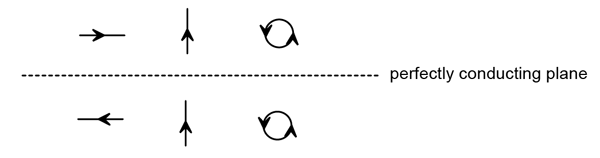
Figure 6. Current sources and their images in a conducting plane.
Example 2: Estimating the Radiated Field from a Small, Low-Impedance Circuit
Suppose the load impedance in the previous example had been only 50 ohms, and the circuit employed a solid plane for the current return path as illustrated in Figure 7. We'll further suppose that the dimensions of the ground plane are 10 cm x 10 cm. Would the emissions from this circuit exceed the FCC Class B limit?
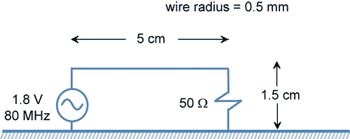
Figure 7. A 50-ohm circuit.
The 50-ohm load resistance is less than the 377-ohm intrinsic impedance of free space, so we use the lower equation in (19). We also need to determine whether or not the inductance of the circuit is limiting the current.
To calculate the inductance of a half-loop above a ground plane, we can replace the ground plane with the image of the half-loop. In this case, we have a virtual loop that is 5 cm x 3 cm as illustrated in Figure 8.
Figure 8. The wire half-loop and its image.
Applying our equation for the inductance of a rectangular wire loop, we note that the inductance of the 5 cm x 3 cm loop is loop is 114 nH. The inductance of the half-loop above the plane is then half this value or 57 nH. This corresponds to a reactive loop impedance of 29 ohms at 80 MHz.
Although we are able to apply image theory to calculate the inductance of the loop, we cannot use image theory to calculate the radiation from the circuit. The ground plane's dimensions are small relative to a wavelength and therefore, the plane looks more like a wide conductor than an infinite plane. We don't have an expression for the radiation from circuits with wide conductors, but if we just want to get a rough estimate, we can apply Equation (19),
. (21)
Note that we use the actual loop area of the circuit and do not adjust our calculation to account for the circuit's plane. If we add 6 dB to this estimate to account for making the measurement in a semi-anechoic environment, we estimate the radiation to be about 62 dB(μV/m) or about 22 dB above the FCC Class B limit.
Input Impedance and Radiation Resistance
In general, if a time-varying voltage appears between any two conducting objects in an open environment, time-varying currents will flow on these conductors and radiation will result. The electrically small circuits described in the previous section are relatively inefficient sources of electromagnetic radiation. Larger resonant structures can produce radiated fields that are many orders of magnitude stronger when driven with the same source voltages.

Figure 9. A simple antenna geometry.
Consider the basic antenna structure illustrated in Figure 9. A sinusoidal voltage source connected between two metal bars draws charge off one bar and pushes it onto the other bar when the voltage is positive. One half cycle later, the polarity is reversed and the charge distribution is inverted. The moving charge results in a current. The ratio of the voltage to the current through the source is the input impedance of the antenna, which in general has a real and imaginary part,
. (22)
At low frequencies, the amount of charge the bars can hold for a given voltage is determined by the mutual capacitance between the bars. In this case, the imaginary part of the input impedance is,
(23)where f is the source frequency and C is the mutual capacitance. If the bars are good conductors, at low frequencies and very little real power is delivered by the source.
However, as the frequency increases (and the bar looks longer relative to a wavelength), several factors combine to change the antenna input impedance:
- The inductance associated with the currents flowing in the bars (and the associated magnetic fields) begin to affect the reactive part of the input impedance;
- The resistive losses increase due to the skin effect;
- Power is lost to radiation which contributes to the real part of the input impedance.
It is convenient to express the real part of the input impedance as the sum of two terms,
(24)
where Rrad is the radiation resistance of the antenna and Rdiss is the loss resistance. The power radiated can then be calculated as,
(25)
and the power dissipated as heat can be calculated as,
. (26)
The ratio of the power radiated to the total power delivered to the structure is called the radiation efficiency and can be calculated using the following equation,
. (27)
Example 3: Radiation Efficiency of an Electrically Small Circuit
Calculate the radiation efficiency of the 5-cm x 2-cm 500-ohm circuit in Figure 5.
We'll start by calculating the power dissipated. If we assume that the power is primarily dissipated in the load resistor (as opposed to the wires), the dissipated power is simply,
. (28)
To estimate the power radiated, we note that the maximum electric field strength at 3 meters is 134 μV/m (as calculated in Example 1). The maximum radiated power density is therefore,
. (29)
This is the maximum power density radiated in any direction, so we can calculate an upper bound on the radiated power by assuming that this power density is radiated in all directions and integrating over a sphere with a 3-meter radius,
. (30)
Therefore, the radiation efficiency of the circuit is,
. (31)
Note that the input impedance of an antenna structure may depend on the antenna environment as well as the size and shape of the antenna. For example, the radiation resistance and the radiated power of any antenna will drop to zero if the antenna is operated in a fully-shielded resonant enclosure.
The Resonant Half-Wave Dipole
An antenna consisting of two simple conductors driven relative to each other by a single source is called a dipole antenna. A thin-wire antenna driven by a source at its center is called a center-driven dipole. The input impedance of a center-driven dipole is plotted in Figure 10 as a function of its electrical length (l/λ).
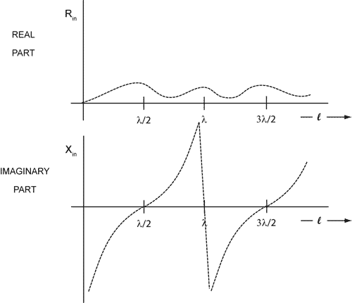
Figure 10. Input impedance of a center-driven dipole.
At very low frequencies (where l << λ), the input impedance is almost entirely reactive and inversely proportional to frequency . However, note that as the length (or frequency) increases, the magnitude of the negative reactance becomes smaller and eventually passes through zero before becoming positive and continuing to increase.
The reactance is zero when the total length of the wire is slightly less than one-half wavelength. A dipole antenna with this length has a real input impedance of approximately 70 ohms and is called a half-wave resonant dipole.
Quiz Question
Calculate the power radiated by a lossless half-wave resonant dipole driven by a 1.0-volt source.
This is a very simple calculation, since both the input resistance and the radiation resistance are about 72 ohms. The correct solution is,
. (32)
To find the maximum radiated field strength at 3 meters from this antenna, we first determine the maximum radiated power density,
. (33)
where is the average power density and D0=1.64 is the directivity of a half-wave dipole antenna.
The maximum radiated electric field can then be calculated using Equation (29) in reverse,
. (34)
Comparing this to the field strength radiated by the electrically small circuit in Figure 5, we can gain an appreciation for just how important the size and shape of the antenna can be. In this case, if we assume both structures were driven at 80 MHz, the maximum dimension of the circuit was 5 cm while the maximum dimension of the dipole is 187.5 cm (half a wavelength at 80 MHz). This is a factor of 37.5. However, the radiated emissions increased by a factor of or 66 dB.
Example 5: Radiation Efficiency of a Half-Wave Dipole
Calculate the radiation efficiency of a center-driven half-wave resonant dipole made from copper wire with a radius (r=0.5 mm) at 100 MHz.
The power radiated by resonant half-wave dipole is simply,
(35)
where I is the current at the source. To calculate the power dissipated, we start by determining the resistance per unit length of the copper wire at 100 MHz.
. (36)
The total power dissipated in the half-wave dipole is then,
. (37)
Therefore, the efficiency of this resonant half-wave dipole is,
. (38)
Compare this to the efficiency of the small circuit in Example 3. Resonant length wire antennas tend to be very efficient compared to electrically small antennas. They can easily be 4 to 6 orders of magnitude more efficient.
Quarter-Wave Monopoles
Half-wave dipoles make good antennas for many applications, but they are large at low frequencies and may not operate as intended close to a large metal surface. A quarter-wave monopole is simply half of a half-wave dipole driven relative to a large metal plane as illustrated is Figure 11. The lower half of the monopole can be modeled as the image of the upper half. Therefore the radiating properties of the quarter-wave monopole are similar to those of the half-wave dipole. The input impedance of a resonant quarter-wave monopole is exactly half that of a resonant half-wave dipole or about 36 ohms.
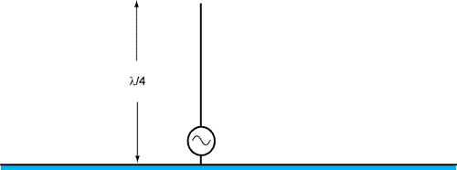
Figure 11. A quarter-wave monopole.
Cables driven relative to large metallic enclosures can often be modeled as monopole antennas. Since resonant monopole antennas are very efficient radiation sources, it is important to ensure that voltages between cables and enclosures be held to very small values at frequencies that might be near cable resonances.
Quiz Question
At approximately what frequency does a 25-cm wire attached to a large metal structure look like a quarter-wave monopole antenna?
The exact answer depends on the orientation of the wire, the cross section of the wire, the structure's size and shape, and other factors. However, 25 cm is a quarter wavelength at 300 MHz. The cable is likely to resonate and become an efficient antenna near this frequency.
Dipoles Driven Off-Center
When a wire antenna is driven off-center, it will still exhibit a resonance near the frequency where it is a half-wavelength long. However, the radiation resistance at resonance will be a function of the source location. Figure 12 plots the radiation resistance of a resonant half-wave dipole as a function of source location. Note that the resistance quickly increases as the source is moved away from the center. A voltage source located near the end of the wire cannot deliver power effectively to the antenna even at resonance.
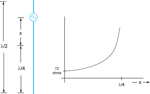
Figure 12. Radiation resistance of a resonant half-wave dipole as a function of source position.
Characteristics of Efficient and Inefficient Antennas
Most of the unintentional radiation sources that an EMC engineer encounters can be modeled as simple dipole antennas. There are basically 3 conditions that have to be met in order for these antennas to radiate effectively:
- The antenna must have two parts;
- both parts must not be electrically small;
- something must induce a voltage between the 2 parts.
The first condition is important to remember when trying to track down the source of a radiation problem. It is not correct to say that a particular wire or a particular piece of metal is the antenna. A single conductor will not be an effective antenna unless it is driven relative to something else. The "something else" is an equally important part of the antenna. Once identified, options for reducing radiated emissions normally become clearer.
Locating the two parts of an effective antenna becomes much easier when we recognize the second condition. For example, if we are looking for the "antenna" responsible for radiated emissions at 50 MHz (λ = 6 meters), then we are looking for 2 conducting objects on the order of a meter long. It is unlikely that these antenna parts are located on the printed circuit board. Most table-top size products can only radiate effectively at low frequencies by driving one cable relative to another. At frequencies below a few hundred MHz, the number of possible antenna parts is limited and often readily apparent without a detailed examination of the entire design.
The third condition above suggests a method for controlling radiated emissions. Once the possible antenna parts have been identified, a device will not generate significant radiated emissions if the voltage between these parts is kept low. This is best accomplished by locating these parts near each other and ensuring that no high-frequency circuits come between them. Tying them together electrically with a good high-frequency connection will further ensure that they are held to the same potential.
Quiz Question
For each pair of antennas illustrated in Figure 13, which antenna in the pair radiates the most?
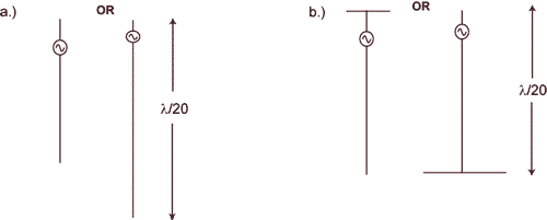
Figure 13. Antenna configurations.
The key to answering this question is to examine each antenna and identify the two antenna parts that are driven by the indicated voltage source. Since at least one part of every antenna is electrically small, it is the smallest part that will limit the overall effectiveness of the antenna.
In Figure 13(a), the short upper wire on the antenna on the right is most limiting; therefore the antenna on the left is more effective. In Figure 13(b), an extra piece of wire has been added to each of the antennas in Figure 13(a). The short upper wire on the antenna on the right is again the most limiting, so the antenna on the left is still more effective. Note that adding to the shorter half of an electrically small antenna has a much greater impact on the antenna efficiency than adding to the larger half.
Slot Antennas
Slot antennas are another potentially efficient type of antenna that EMC engineers should be familiar with. As illustrated in Figure 14, a slot antenna is formed by a long thin aperture in a conducting surface. An electric field distribution appearing in the slot (e.g. due to a surface current that is disrupted by the slot) produces a radiated field in the same way that a current distribution on a wire does. In fact, slot antennas are generally analyzed by replacing the electric field distribution with an equivalent (but fictitious) magnetic current and solving for the fields radiated by these magnetic currents. The fields radiated by a resonant half-wave slot have the same form (with the role of E and H reversed) as the fields from a resonant half-wave dipole. Like wire antennas, electrically small slots are inefficient antennas, while slots approaching a half-wavelength can be very efficient.
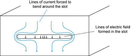
Figure 14. Slot antenna.
Receiving Antennas
Generally speaking, the same structures that make good radiating antennas also make good receiving antennas. For this reason, many of the same techniques used to identify or prevent radiated emission problems can be applied to radiated susceptibility problems. However unlike radiation, where the source impedance is almost always low relative to the antenna input impedance, the devices that exhibit susceptibility problems often have high impedance inputs. Because of this, it is not necessarily true that higher antenna input impedances correspond to poorer antenna performance.
The power received by a device connected to a dipole antenna can be calculated using the following formula,
. (39)
where
is the power density of the incident wave,
is the effective aperture of the antenna,
is the factor accounting for the impedance mismatch between the antenna and the receiver, and
is the voltage reflection coefficient at the receiver.
This formula may be difficult to apply in many situations however, because it requires significant information about both the antenna and the receiver. If an order-of-magnitude approximate solution is good enough, it is convenient to estimate the maximum voltage dropped across a higher impedance input as,
. (40)
where lant is the length of the dipole antenna or one half-wavelength, whichever is greater.
Example 6: Estimating the Maximum Voltage Coupled to a Half-Wave Dipole Antenna
Compare the actual maximum voltage coupled to a 500-ohm receiver from a half-wave dipole to the estimate in Equation (40).
If we assume that the receiver is positioned at the point on the dipole where its impedance is matched to the radiation resistance, the expression for the received power becomes,
. (41)
The received voltage is,
. (42)
We can compare this to the estimated value,
(43)
and note that the estimate was accurate to within 2 dB in this case.
Example 7: Estimating the Maximum Voltage Coupled to an Electrically Short Dipole Antenna
Compare the actual maximum voltage coupled to a matched receiver from an electrically short dipole to the estimate in Equation (40).
The radiation resistance of an electrically short dipole antenna is approximately,
. (44)
The directivity, D0, is 1.5. The received power can be readily calculated as,
. (45)
The received voltage is therefore,
. (46)
We can compare this to the estimated value,
. (47)
In this case, the voltage is over-estimated by a factor of 4 (12 dB).